Array substrate and manufacturing method thereof

A technology of array substrates and bases, which is applied in the direction of electrical components, electric solid devices, circuits, etc., can solve the problem of a large number of manufacturing processes, and achieve the effect of reducing the number of photomasks and manufacturing processes

Active Publication Date: 2020-10-09
WUHAN CHINA STAR OPTOELECTRONICS SEMICON DISPLAY TECH CO LTD
View PDF3 Cites 3 Cited by
  • Summary
  • Abstract
  • Description
  • Claims
  • Application Information

AI Technical Summary

Problems solved by technology

[0004] The embodiment of the present application provides an array substrate and its manufacturing method to solve the problem of a large number of photomasks and manufacturing processes caused by the fact that the LTPS TFT and the Oxide TFT are not on the same layer of the existing LTPO array substrate

Method used


Image

  • Array substrate and manufacturing method thereof
  • Array substrate and manufacturing method thereof
  • Array substrate and manufacturing method thereof

Examples


Embodiment 1

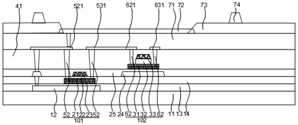
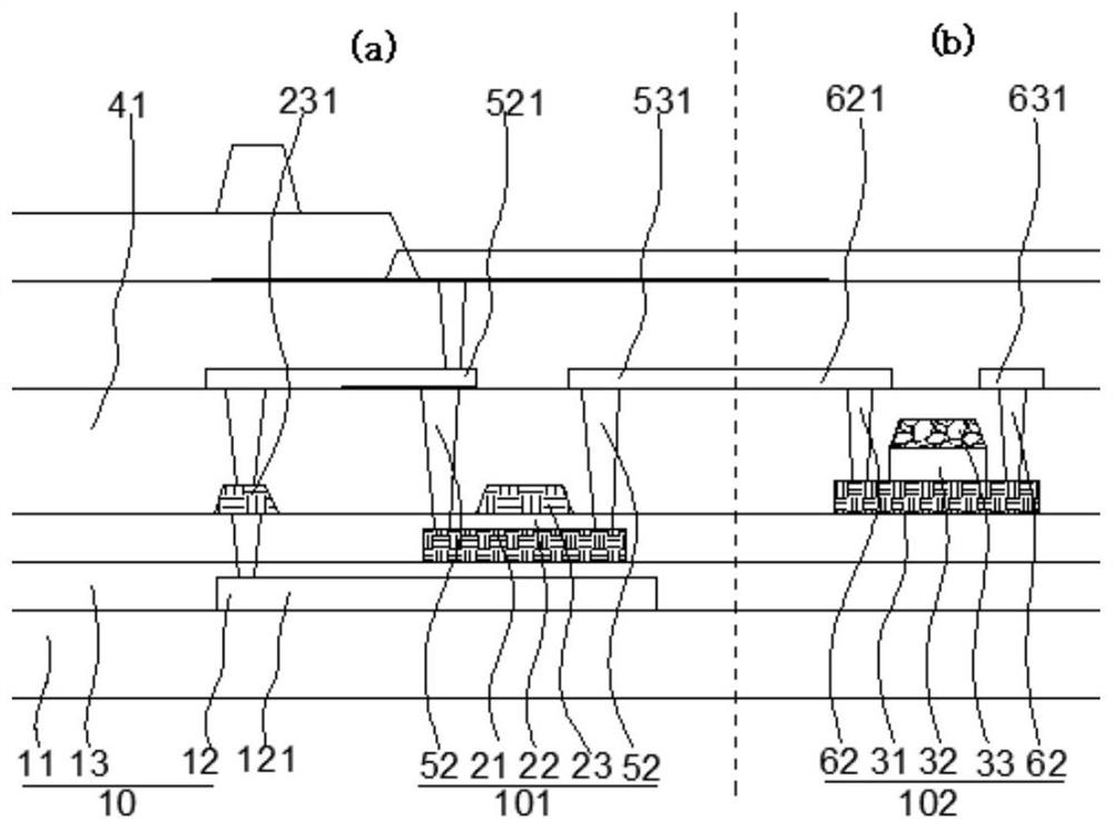
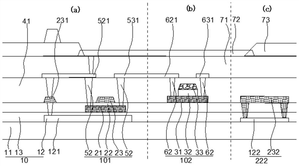
[0041] see figure 2 As shown, an array substrate includes: a substrate 10; a first TFT 101 located in the region (a) is disposed on the substrate, and the first TFT 101 includes a first active layer 21 disposed on the substrate, disposed on The first gate insulating layer 22 on the substrate 10 and the first active layer 21 and covering the first active layer 21 , and the first gate disposed on the first gate insulating layer 22 electrode 23; the second TFT102 located in the (b) region is disposed on the first gate insulating layer 22, and the second TFT102 includes a second active active layer disposed on the first gate insulating layer 22 layer 31 , a second gate insulating layer 32 disposed on the second active layer 31 , and a second gate 33 disposed on the second gate insulating layer 32 .

[0042] Wherein the material of the first gate 23 is the same as that of the second active layer 31 , and is an integrally formed structure. The material of the second active layer ...

Embodiment 2

[0046] see image 3 , this embodiment is the same or similar to Embodiment 1, the difference is:

[0047] The array substrate further includes signal sub-lines 232 located in the region (c). The material of the signal sub-line 232 is the same as that of the first gate 23 and the second active layer 31 , and is an integrally formed structure. Specifically, the signal sub-line 232 can be formed at the same time as the second active layer 31 and the first gate 23 are formed, and the formation method includes but is not limited to: first forming the entire surface of the oxide semiconductor film layer , and then simultaneously form the patterned first gate 23 , the second active layer 31 , and the signal sub-lines 232 through processes such as exposure and etching. In some embodiments, in order to reduce the resistance value of the first gate 23 and the signal sub-line 232 made of oxide semiconductor, it can be processed by Plasma, such as N2, He, N2O, H2, etc. or their mixed ga...

Embodiment 3

[0053] see Figure 5 , this embodiment is the same or similar to Embodiment 1 to Embodiment 2, the difference is that:

[0054] The multifunctional metal layer 12 also includes a capacitive sublayer 123 on the substrate 11, and the first gate insulating layer 22 is provided with a first capacitive electrode 331 corresponding to the capacitive sublayer 123, The first gate insulating layer 22, the first gate 23, the second TFT 102, and the first capacitance electrode 331 are provided with a cover covering the first gate insulating layer 22, the first gate 23. The second TFT 102 , the first and the interlayer insulating layer 41 of the capacitor electrode 331 , the interlayer insulating layer 41 is provided with a second capacitor electrode 531 corresponding to the first capacitor electrode 331 .

[0055] The first capacitor electrode 331 is made of the same material as the second gate 531 , and is integrally formed. Specifically, the formation method includes but is not limite...


PUM


Abstract

The invention provides an array substrate and a manufacturing method thereof. The array substrate comprises a base, a first TFT and a second TFT, wherein the first TFT is arranged on the substrate, and the first TFT comprises a first active layer arranged on the substrate, a first gate insulation layer arranged on the substrate and the first active layer and covering the first active layer, and afirst gate arranged on the first gate insulation layer; the second TFT is arranged on the first gate insulating layer, and the second TFT comprises a second active layer arranged on the first gate insulation layer, a second gate insulation layer arranged on the second active layer and a second gate arranged on the second gate insulation layer; and the first gate and the second active layer are made of the same material, and the first gate and the second active layer are integrally formed.

Description

technical field [0001] The present application relates to the field of display technology, in particular to an array substrate and a manufacturing method thereof. Background technique [0002] In the field of display technology today, liquid crystal displays (Liquid Crystal Display, LCD) and organic light emitting diode displays (Organic Light Emitting Diode, OLED) have been widely used in daily life, such as mobile phones or televisions. [0003] At present, most OLED displays use LTPS (Low Temperature Poly-silicon low temperature polysilicon) TFT (Thin Film Transistor, thin film transistor) panel technology. After several years of improvement, although LTPS display panels have been welcomed by the market, they have the disadvantages of high production costs and high power consumption. Therefore, technicians have developed LTPO (Low Temperature Polycrystalline Oxide, low temperature Polycrystalline oxide) display panel technology, that is, the LTPO display panel obtained b...

Claims


Application Information

Patent Timeline
Patent Type & Authority Applications(China)
IPC IPC(8): H01L27/12H01L27/32
CPCH01L27/1214H01L27/124H01L27/1222H01L27/1259H01L27/1288H10K59/12
Inventor 龚吉祥张毅先鲜于文旭
Owner WUHAN CHINA STAR OPTOELECTRONICS SEMICON DISPLAY TECH CO LTD
Why Eureka
Try Eureka