Image sensor and forming method of image sensor pixel structure

An image sensor and pixel structure technology, applied in the field of semiconductors, can solve the problems of low electron transmission rate deep in the photodiode, small surface channel and vertical channel path, etc., to increase the area of ​​electron transmission and communication, reduce electron residue, The effect of increasing the transport rate of photogenerated electrons

Pending Publication Date: 2020-10-16
SHANGHAI HUALI MICROELECTRONICS CORP
View PDF4 Cites 1 Cited by
  • Summary
  • Abstract
  • Description
  • Claims
  • Application Information

AI Technical Summary

Problems solved by technology

[0005] The purpose of the present invention is to provide a method for forming an image sensor pixel structure, so as to solve the problem that the surface channel and the vertical channel path are relatively small in the existing image sensor pixel structure, resulting in a low electron transmission rate deep in the photodiode

Method used


Image

  • Image sensor and forming method of image sensor pixel structure
  • Image sensor and forming method of image sensor pixel structure
  • Image sensor and forming method of image sensor pixel structure

Examples


Embodiment Construction

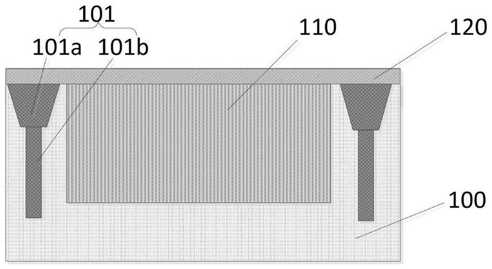
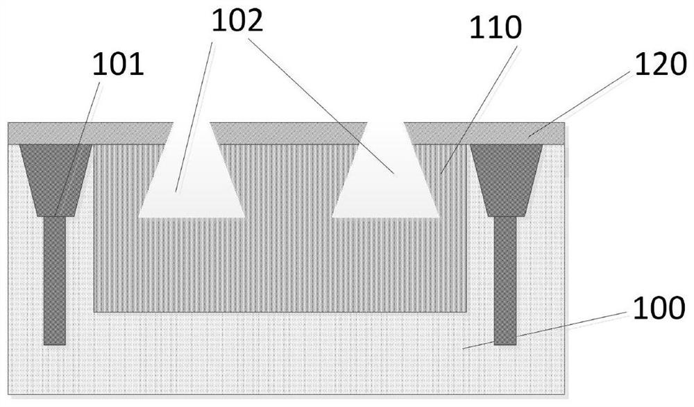
[0040] As mentioned in the background art, for an image sensor with a small pixel, since the pixel is small, photons are converted into fewer electrons, and the charge in the full well is on the order of thousands. At present, the surface channel and the vertical channel are relatively small in the way of electron transmission, and the transmission of electrons deep in the photodiode needs to pass through the entire junction region, which is easy to be recombined, resulting in low extraction efficiency. Moreover, electrons deep in the P-N junction need a certain amount of time and voltage to complete the transmission, which is not conducive to fast reading.

[0041] For this reason, the present invention provides a method for forming an image sensor pixel structure to solve the problem that the surface channel electricity and vertical channel electron transmission paths in the image sensor pixel structure are relatively small, resulting in low electron transmission rates deep i...


PUM

PropertyMeasurementUnit
sizeaaaaaaaaaa
radiusaaaaaaaaaa

Abstract

The invention provides an image sensor and a forming method of an image sensor pixel structure, and is applied to the technical field of semiconductors. A part of a gate structure of a transmission transistor in a pixel structure is expanded into a photodiode region in a semiconductor substrate by forming a trench, so that the width of the photodiode can be extended in the transverse direction while the effective area of the gate structure of the transmission transistor is increased, the electron transmission communication area is increased, the photo-induced electron transmission rate is improved, the electron residue at the bottom of the diode is reduced, and the full-well capacity of the photodiode is finally improved. The manufacturing cost of the chip can be reduced under the condition that the area and lighting of the chip are not influenced. In addition, due to the fact that the electron transmission communication area in the pixel structure is increased, electron residues at the bottom of the diode are reduced, and therefore white pixels are reduced.

Description

technical field [0001] The invention relates to the field of semiconductor technology, in particular to an image sensor and a method for forming a pixel structure of the image sensor. Background technique [0002] CMOS image sensors have developed rapidly in the past ten years, and are now widely used in mobile phones, computers, digital cameras and other fields. Generally, an active pixel unit of a CMOS image sensor includes a photodiode (Photo Diode, PD) and several transistors located in the epitaxial layer. Taking a 4T structure CMOS image sensor as an example, the four transistors specifically include a transfer tube 110 (Transfer, Tx) , Source follower tube (Source Follow, SF), reset tube (Reset, RST) and row selection tube (Row Select, RS). Among them, the basic working principle of the CMOS image sensor is as follows: before lighting, turn on the reset transistor and transfer transistor to release the original electrons in the photodiode area; when the light is on, ...

Claims


Application Information

Patent Timeline
Patent Type & Authority Applications(China)
IPC IPC(8): H01L27/146
CPCH01L27/14683H01L27/1463H01L27/14603H01L27/14643
Inventor 黄斌冰张磊王奇伟陈昊瑜顾珍董立群
Owner SHANGHAI HUALI MICROELECTRONICS CORP
Why Eureka
Try Eureka