
Memory structure and manufacturing method thereof

A manufacturing method and memory technology, applied in the field of memory, capable of solving problems such as easy interference of leads

Inactive Publication Date: 2020-10-27
NAT CENT FOR ADVANCED PACKAGING
View PDF5 Cites 0 Cited by
  • Summary
  • Abstract
  • Description
  • Claims
  • Application Information

AI Technical Summary

Problems solved by technology

[0003] Therefore, the present invention solves the problem that memory chips are interconnected by bonding wires in the prior art, and leads are easily interfered with, thereby providing a memory structure and a manufacturing method thereof

Method used


Image

  • Memory structure and manufacturing method thereof
  • Memory structure and manufacturing method thereof
  • Memory structure and manufacturing method thereof

Examples


Embodiment 1

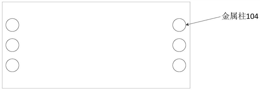
[0036] An embodiment of the present invention provides a memory structure, including: a plurality of memory units with the same structure. Multiple storage units with the same structure are stacked to form a stacked structure. Each storage unit has the same structure, such as Figure 3-5 As shown, the specific storage unit 10 includes: a storage module 101, the upper part and the surrounding of the storage module 101 are covered with a plastic sealing layer 102, the bottom of the storage module 101 is provided with a connector 103, and the side of the storage module 101 is provided with a metal The post 104, the connecting piece 103 extends to the side of the storage module 101, and is electrically connected to the metal post 104; the connecting piece 103 is also the RDL line of the storage module, and is used to connect to other storage modules. An RDL line makes an input / output (I / O) connection point of the semiconductor package available at another location, wherein the RD...

Embodiment 2

[0050] An embodiment of the present invention provides a memory manufacturing method, which is used to manufacture the memory structure described in Embodiment 1 of the invention above, specifically, as Figure 9-12 As shown, the memory manufacturing method includes:

[0051] Step S301, generating a plastic sealing layer covering the storage module on the storage module;

[0052] Step S302, assembling a connector extending to the side of the storage module at the bottom of the storage module;

[0053] Step S303, assembling a metal post electrically connected to the connector on the side of the storage module to obtain a storage unit;

[0054] Step S304, pasting an insulating film on the bottom of the storage unit, and placing the storage unit on another storage unit with the same structure;

[0055] Step S305, heating and pressurizing the insulating film, so that the insulating film is melted to form an insulating material layer, which fills the gap between the upper and low...


PUM


Abstract

The invention discloses a memory structure and a manufacturing method thereof. The memory structure comprises a plurality of storage units with the same structure; each storage unit comprises a storage module, a plastic package layer covers the storage module, a connecting piece is arranged at the bottom of the storage module, a metal column is arranged on the side edge of the storage module, andthe connecting piece extends to the side edge of the storage module and is electrically connected with the metal column; the plurality of storage units with the same structure are stacked, and the storage units positioned at the lower part are electrically connected with the connecting pieces of the storage units positioned at the upper part through the metal column. According to the invention, the capacity of the memory is expanded by stacking the memory modules, external leads are not needed, the interference among the leads is avoided, the manufacturing of the high-capacity memory is realized without a complex packaging process, complex chip assembly equipment is not needed, the packaging process is simple, and the cost is low.

Description

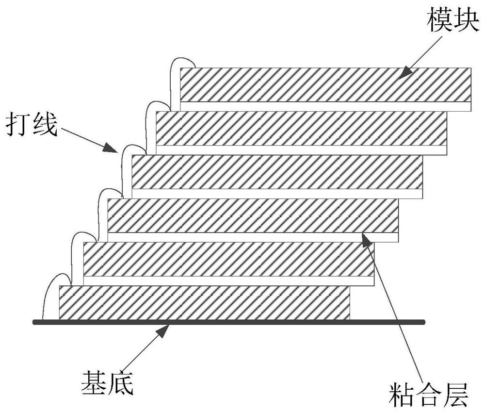
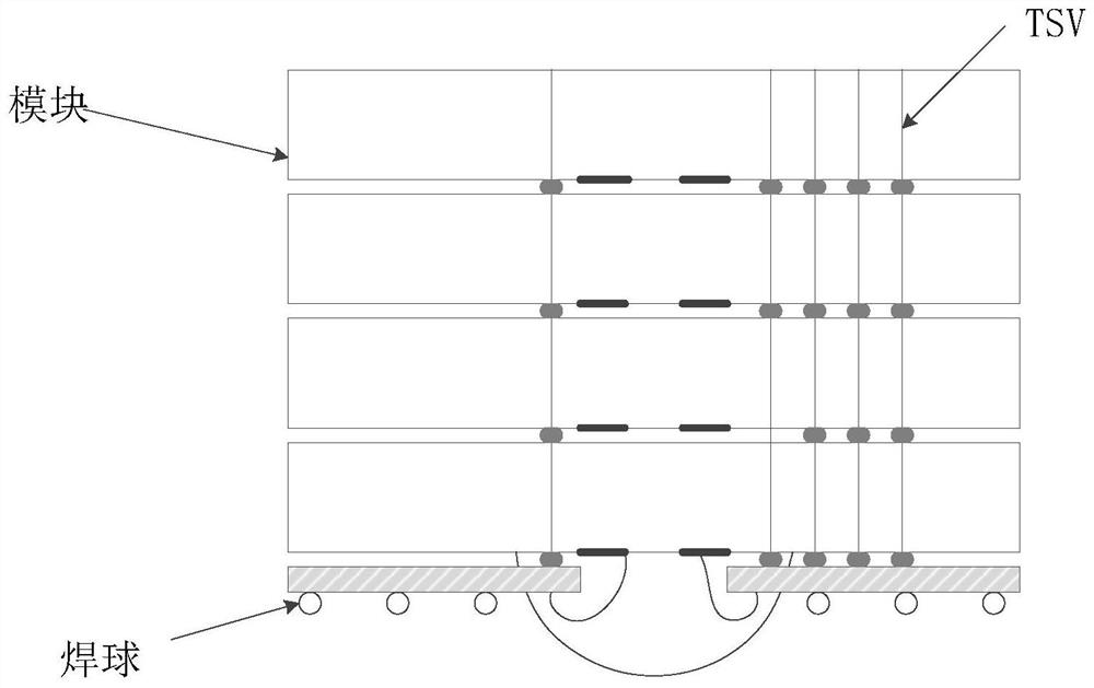
technical field [0001] The invention relates to the field of memory technology, in particular to a memory structure and a manufacturing method thereof. Background technique [0002] In the technical field of memory, the memory capacity is usually expanded by stacking memory modules. With the advent of the digital age, there is a greater and greater demand for data storage, which also leads to an increasing demand for memory capacity. In the prior art, for memory expansion methods, taking NAND Flash packaging as an example, it is generally divided into two types: one is to superimpose memory chips (memory modules) and interconnect them by bonding, so as to increase the overall capacity of the memory, such as figure 1 As shown, but the interconnection between the memory chips is long, and the leads are easy to interfere; the other is to directly interconnect the NAND Flash chips through silicon vias (Through Silicon Via, TSV), such as figure 2 shown. However, NAND Flash ch...

Claims


Application Information

Patent Timeline
IPC IPC(8): H01L23/485H01L21/60H01L21/56H01L25/18H01L21/50
CPCH01L23/4824H01L24/03H01L21/56H01L25/18H01L25/50H01L2224/0231H01L2224/02331H01L2224/02381H01L2224/73207H01L2224/48145H01L2224/73265H01L2224/48091H01L2224/16145H01L2224/32145H01L2924/15311H01L2224/4824H01L2224/83191H01L2924/00014H01L2924/00012
Inventor 陈立军曹立强姚大平
Owner NAT CENT FOR ADVANCED PACKAGING
Learn More