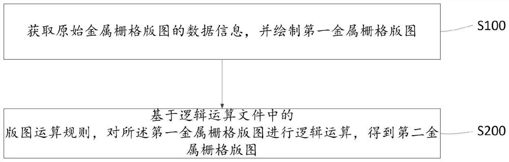
Method for generating metal grid layout of image sensor and metal grid photomask pattern
An image sensor, metal grid technology, applied in the direction of electric solid-state devices, semiconductor devices, electrical components, etc., can solve the problem of high cost
- Summary
- Abstract
- Description
- Claims
- Application Information
AI Technical Summary
Problems solved by technology
Method used
Image


Examples
Embodiment Construction
[0040] The specific implementation manner of the present invention will be described in more detail below with reference to schematic diagrams. The advantages and features of the present invention will be more apparent from the following description. It should be noted that all the drawings are in a very simplified form and use imprecise scales, and are only used to facilitate and clearly assist the purpose of illustrating the embodiments of the present invention.
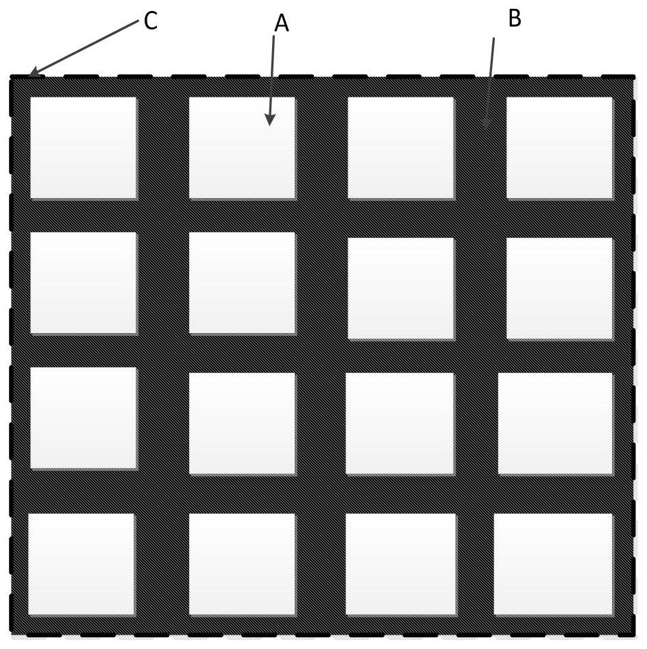
[0041] As mentioned in the background technology, in the current generation method of the special-shaped metal grid layout of the image sensor, the layout design engineer needs to use the layout drawing software that mainly supports standard graphics to draw through complicated drawing operation steps, therefore, This increases the design time and cost of layout design engineers, reduces the efficiency of layout design and generation, and makes it inconvenient to realize the diversity of layouts during the research...
PUM
 Abstract
Description
Claims
Application Information
 - R&D Engineer
- R&D Manager
- IP Professional
- Industry Leading Data Capabilities
- Powerful AI technology
- Patent DNA Extraction
Browse by: Latest US Patents, China's latest patents, Technical Efficacy Thesaurus, Application Domain, Technology Topic.
© 2024 PatSnap. All rights reserved.Legal|Privacy policy|Modern Slavery Act Transparency Statement|Sitemap