Modular crucible device for silicon carbide crystal growth and growth method thereof

A technology of crystal growth and silicon carbide, applied in the direction of crystal growth, single crystal growth, single crystal growth, etc., which can solve the problems that are not conducive to the preparation of high-quality single crystals, environmental changes, and the speed of process optimization

Inactive Publication Date: 2020-10-30
哈尔滨科友半导体产业装备与技术研究院有限公司
View PDF3 Cites 3 Cited by
  • Summary
  • Abstract
  • Description
  • Claims
  • Application Information

AI Technical Summary

Problems solved by technology

[0002] When using the PVT method to prepare silicon carbide (SiC) single crystals, the crucible made of high-temperature resistant materials provides a relatively closed space for the reaction and deposition of gas phase components. The crucible often needs to be heated above 2000°C for more than 100 hours. Silicon carbide crystals are obtained from the powder, and the raw materials in the crucible gradually decrease with the formation of single crystals, which leads to changes in the environment of the thermal field, and cannot obtain a stable thermal field for long crystals, resulting in uneven reaction and deposition of gas phase components, which cannot To meet the requirement of process optimization to adjust the thermal field at any time, to a certain extent, the speed of process optimization is limited, which is not conducive to the preparation of high-quality single crystal

Method used


Image

  • Modular crucible device for silicon carbide crystal growth and growth method thereof

Examples


specific Embodiment approach 1

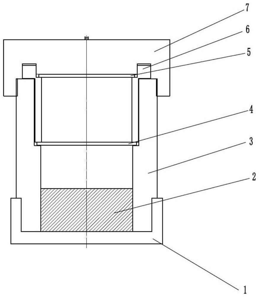
[0023] A modular crucible device for growing silicon carbide crystals, the described modular crucible device for growing silicon carbide crystals includes a crucible bottom 1, the crucible bottom is connected to a crucible body 3, and the crucible body The upper end of the crucible is provided with a crucible support 6, the upper layer of the crucible support is placed with a seed crystal 5, the lower layer of the crucible support is placed with a silicon carbide polycrystalline block 4, the bottom of the crucible body is placed with a silicon carbide powder 2, and the crucible cover 7 is connected to the crucible. Body cover.

[0024] A modular crucible device for silicon carbide crystal growth described in this embodiment, the crucible bottom and the crucible body are connected by bolts, the crucible body and the crucible support are connected by bolts, The crucible cover and the crucible body are connected by bolts.

[0025] In the modularized crucible device for silicon c...

specific Embodiment approach 2

[0032] According to the first embodiment, a silicon carbide crystal growth method of a modular crucible device for silicon carbide crystal growth includes the following steps:

[0033] Step 1. Assemble a modular crucible device for silicon carbide crystal growth. The crucible bottom and crucible body of a modular crucible device for silicon carbide crystal growth are tightly connected by graphite bolts, and then the silicon carbide powder is loaded into the described modular crucible device for silicon carbide crystal growth, then the crucible body and the crucible support are tightly connected by graphite bolts, and then the silicon carbide polycrystalline block is placed on the lower layer of the crucible support, and the The seed crystal is placed on the upper layer of the crucible support, and then the crucible cover and the crucible body are tightly connected by graphite bolts;

[0034] Step 2. Put a modular crucible device assembled in step 1 for the growth of silicon ca...

specific Embodiment approach 3

[0037] A modular crucible device for growing silicon carbide crystals, the described modular crucible device for growing silicon carbide crystals includes a crucible bottom 1, the crucible bottom is connected to a crucible body 3, and the crucible body The upper end of the crucible is provided with a crucible support 6, the upper layer of the crucible support is placed with a seed crystal 5, the lower layer of the crucible support is placed with a silicon carbide polycrystalline block 4, the bottom of the crucible body is placed with a silicon carbide powder 2, and the crucible cover 7 is connected to the crucible. Body cover.

[0038] A modular crucible device for silicon carbide crystal growth described in this embodiment, the crucible bottom and the crucible body are connected by bolts, the crucible body and the crucible support are connected by bolts, The crucible cover and the crucible body are connected by bolts.

[0039] In the modularized crucible device for silicon c...


PUM

PropertyMeasurementUnit
thicknessaaaaaaaaaa
diameteraaaaaaaaaa
thicknessaaaaaaaaaa

Abstract

The invention discloses a modular crucible device for silicon carbide crystal growth and a growth method thereof, belonging to the field of silicon carbide crystal growth devices. The technical problem to be solved by the invention is how to provide a stable crystal growth thermal field. The device comprises a crucible bottom, wherein the crucible bottom is connected with a crucible body, a crucible support is arranged at the upper end of the crucible body, seed crystals are placed on the upper layer of the crucible support, silicon carbide polycrystalline blocks are placed on the lower layerof the crucible support, silicon carbide powder is placed at the inner bottom of the crucible body, and a crucible cover covers the crucible body. The device disclosed by the invention is modularized,can be properly combined according to actual requirements, allows a more accurate crucible to be obtained and realizes gas diversion in a reaction chamber along with single crystal growth, the silicon carbide polycrystalline blocks in the crucible can be adjusted and repeatedly used, and environmental stability of a crucible thermal field is realized. The device is used for silicon carbide crystal growth.

Description

technical field [0001] The invention belongs to the field of silicon carbide crystal growth devices; in particular, it relates to a modular crucible device for growing silicon carbide crystals and a growth method thereof. Background technique [0002] When using the PVT method to prepare silicon carbide (SiC) single crystals, the crucible made of high-temperature resistant materials provides a relatively closed space for the reaction and deposition of gas phase components. The crucible often needs to be heated above 2000°C for more than 100 hours. Silicon carbide crystals are obtained from the powder, and the raw materials in the crucible gradually decrease with the formation of single crystals, which leads to changes in the environment of the thermal field, and cannot obtain a stable thermal field for long crystals, resulting in uneven reaction and deposition of gas phase components, which cannot Satisfying the need for process optimization to adjust the thermal field at an...

Claims


Application Information

Patent Timeline
Patent Type & Authority Applications(China)
IPC IPC(8): C30B29/36C30B23/00
CPCC30B23/00C30B29/36
Inventor 不公告发明人
Owner 哈尔滨科友半导体产业装备与技术研究院有限公司
Why Eureka
Try Eureka