

Light-emitting device, light wavelength conversion device, and display device
A light-emitting device and light-emitting spectrum technology, which is applied in electroluminescent light sources, identification devices, lighting devices, etc., can solve the problem of narrow half-value width and half-value width, and achieve the effects of high luminous efficiency and wide color reproduction range
- Summary
- Abstract
- Description
- Claims
- Application Information
AI Technical Summary
Problems solved by technology
Method used
Image

Examples
no. 1 approach 〕
[0050] One embodiment of the present invention will be described in detail below. Figure 4 It is a diagram showing the outline of QLED display devices 400a and 400b according to the first embodiment of the present invention. A light-emitting layer including InP-based quantum dots is deposited on the substrate 440 . The blue light emitting layer 410 is preferably made of a ZnSe-based material. The green light emitting layer 420 and the red light emitting layer 430 are preferably made of an InP-based material. The substrate 440 includes light absorbing layers 450, 550 on the face opposite to the face on which the light emitting layer is deposited. The light absorbing layers 450 and 550 preferably selectively absorb light of 570 to 610 nm. The light-absorbing layer 450, 550 involved selectively absorbs light in the range of 570-610 nm to reduce the tail of the above-mentioned luminescence spectrum.
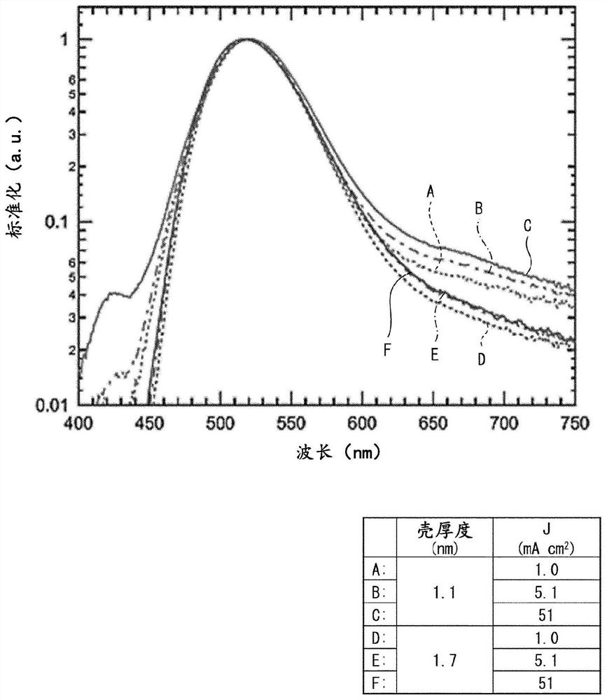
[0051] Figure 5 It is a graph showing the graph of the emission spectrum ...
no. 2 approach 〕
[0064] Next, other embodiments of the present invention will be described. In addition, for convenience of description, members having the same functions as those described in the above-mentioned embodiment are denoted by the same reference numerals, and description thereof will not be repeated.
[0065] although Figure 4 The relationship between the light-emitting layer including InP-based quantum dots and the light-absorbing layer is schematically shown, but the specific configuration of the QLED device will be described in the second embodiment.
[0066] Image 6 It is a cross-sectional view schematically showing QLED devices 600a and 600b according to the second embodiment. Such as Image 6 Like the QLED device 600a shown in (a), the substrate 440 is disposed on the light absorbing layer 450, the first electrode 610 is deposited on the substrate 440, and the hole functional layer and the light emitting layer are sequentially deposited on the first electrode 610 (601 ,...
no. 3 approach 〕
[0073] Next, other embodiments of the present invention will be described. In addition, for convenience of description, members having the same functions as those described in the above-mentioned embodiment are denoted by the same reference numerals, and description thereof will not be repeated.
[0074] Figure 7 It is a cross-sectional view schematically showing QLED devices 700a and 700b according to the third embodiment. Figure 7 The QLED device 700a shown in (a) and Figure 7 700b shown in (b) omits the substrate under the first electrode 610 together. In addition, since the light-absorbing layer does not contribute to the blue quantum dot light-emitting layer, in Figure 7 Only the green light emitting layer 602 is shown in the figure. Since the red light emitting layer 603 is the same as the green light emitting layer 602, in Figure 7 Omit it in .
[0075] when Figure 7 (a) with Image 6 In comparison with (a), the HTL and light absorbing layer 710 is deposit...
PUM
| Property | Measurement | Unit |
|---|---|---|
| full width at half maximum | aaaaa | aaaaa |
Abstract
Description
Claims
Application Information