
Organic light-emitting device and display device

A technology of electroluminescent devices and display devices, applied in the direction of electric solid-state devices, electrical components, semiconductor devices, etc., can solve the problems of efficiency and life decay, reduce current density, avoid efficiency roll-off, and avoid excitons in the light-emitting layer Diffusion effect

Active Publication Date: 2020-11-10
KUNSHAN NEW FLAT PANEL DISPLAY TECH CENT
View PDF10 Cites 3 Cited by
  • Summary
  • Abstract
  • Description
  • Claims
  • Application Information

AI Technical Summary

Problems solved by technology

[0003] However, there are serious efficiency and lifetime decay problems in TASF devices at present

Method used


Image

  • Organic light-emitting device and display device
  • Organic light-emitting device and display device
  • Organic light-emitting device and display device

Examples


Embodiment 1

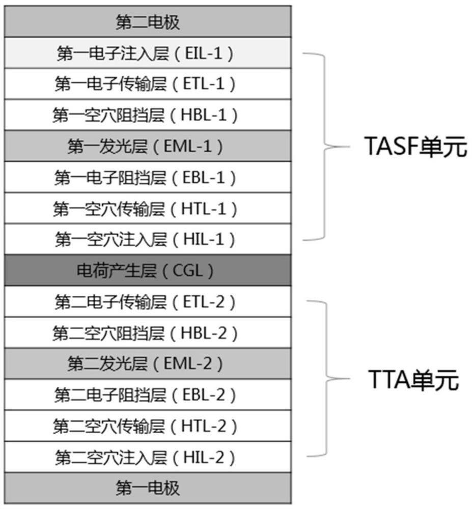
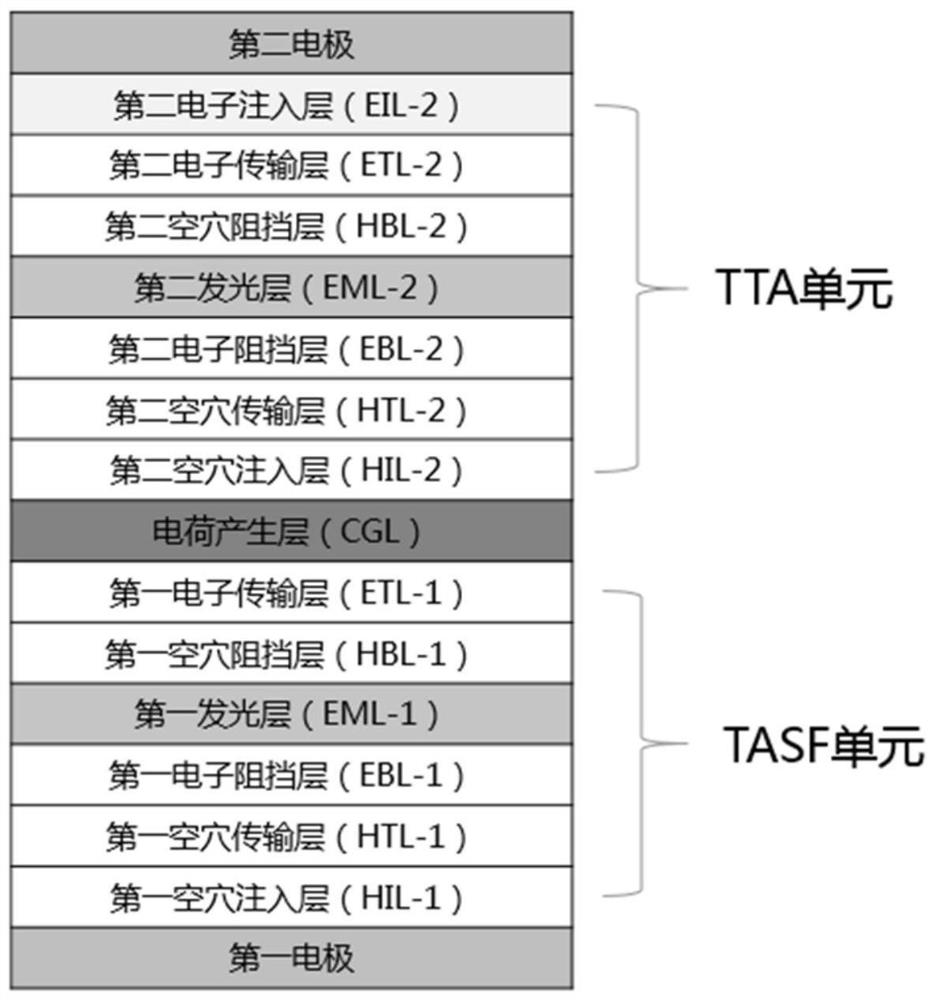
[0096] The invention provides a stacked organic electroluminescent device, the device structure is as follows figure 1 As shown, the first electrode, the TTA unit, the charge generation layer (CGL), the TASF unit and the second electrode are stacked from bottom to top. Among them, the TASF unit includes the first hole injection layer (HIL-1), the first hole transport layer (HTL-1), the first electron blocking layer (EBL-1), the first light emitting layer (EML-1), first hole blocking layer (HBL-1), first electron transport layer (ETL-1) and first electron injection layer (EIL-1). The TTA unit includes a stacked second hole injection layer (HIL-2), a second hole transport layer (HTL-2), a second electron blocking layer (EBL-2), and a second light emitting layer ( EML-2), the second hole blocking layer (HBL-2) and the second electron transport layer (ETL-2).

[0097] The preparation method of the device of this embodiment is as follows:

[0098] (1) The glass plate coated with...

Embodiment 2-9 and 11

[0126] The difference between Examples 2-9 and 11 and Example 1 lies in the types of EML-1 layer materials and EML-2 layer materials, see Table 1 for details, and the rest are the same.

Embodiment 10

[0128] The only difference from Example 1 is that the thickness of the first light-emitting layer is 15 nm.


PUM

PropertyMeasurementUnit
Thicknessaaaaaaaaaa

Abstract

The invention relates to an organic light-emitting device and a display device. The organic light-emitting device comprises a first electrode, a second electrode and at least two organic light-emitting units located between the first electrode and the second electrode, wherein at least two organic light-emitting units are arranged in a stacked manner; at least two organic light-emitting units comprise a first organic light-emitting unit, the first organic light-emitting unit comprises a first light-emitting layer, and the first light-emitting layer contains a first host material, a thermal activation delayed fluorescence sensitizer and a first fluorescent dye. According to the organic light-emitting device provided by the invention, the current density of the device under the same brightness can be remarkably reduced, and relatively high efficiency and relatively long service life can be obtained under the condition of relatively high brightness.

Description

technical field [0001] The invention relates to the technical field of organic electroluminescence, in particular to an organic electroluminescence device and a display device. Background technique [0002] Thermally activated sensitized fluorescence (TASF) means that when thermally activated delayed fluorescence (TADF) materials are used as sensitizers, the energy of the host material is transferred to the TADF material, and then its triplet energy passes through the reverse intersystem crossing (RISC) The process returns to the singlet state, and then the energy is transferred to the doped fluorescent dye to emit light, which can realize the complete energy transfer from the host to the dye molecule, so that the traditional fluorescent doped dye can also break through the 25% internal quantum efficiency limit. [0003] However, there are relatively serious efficiency and lifetime degradation problems in TASF devices at present. Contents of the invention [0004] In view...

Claims


Application Information

Patent Timeline
IPC IPC(8): H01L51/50H01L51/52
CPCH10K85/623H10K85/624H10K85/625H10K85/622H10K85/653H10K85/626H10K85/633H10K85/615H10K85/631H10K85/6574H10K85/6572H10K85/657H10K50/121H10K50/11H10K50/19H10K85/658H10K59/32H10K50/858H10K2101/20H10K2101/30H10K2101/40H10K85/322H10K85/636H10K85/60
Inventor 李国孟席昭洋高孝裕孙磊徐超李梦真
Owner KUNSHAN NEW FLAT PANEL DISPLAY TECH CENT
Learn More