Insulated gate bipolar transistor and manufacturing method thereof

A technology of bipolar transistors and manufacturing methods, applied in semiconductor/solid-state device manufacturing, semiconductor devices, electrical components, etc., can solve device damage, affect threshold voltage stability and uniformity, and the range of lateral diffusion and vertical diffusion is different Easy to control and other issues to achieve the effect of improving the withstand voltage

Active Publication Date: 2020-11-13
SEMICON MFG ELECTRONICS (SHAOXING) CORP +1
View PDF5 Cites 0 Cited by
  • Summary
  • Abstract
  • Description
  • Claims
  • Application Information

AI Technical Summary

Problems solved by technology

Therefore, the junction depth of the PN junction formed by the P-type ring and the N-type substrate is greatly affected by thermal diffusion, and the range of lateral diffusion and vertical diffusion is not easy to control, and the formed PN junction is too shallow or too deep to degrade the device. The withstand voltage of the cell area is prone to snap back, causing irreversible damage to the device; and if the PN junction is too deep, the lateral diffusion is too large, which will affect the stability and uniformity of the threshold voltage (Vth)

Method used


Image

  • Insulated gate bipolar transistor and manufacturing method thereof
  • Insulated gate bipolar transistor and manufacturing method thereof
  • Insulated gate bipolar transistor and manufacturing method thereof

Examples


Embodiment Construction

[0046] In order to make the purpose, advantages and features of the present invention clearer, the insulated gate bipolar transistor and its manufacturing method proposed by the present invention will be further described in detail below. It should be noted that all the drawings are in a very simplified form and use imprecise scales, and are only used to facilitate and clearly assist the purpose of illustrating the embodiments of the present invention.

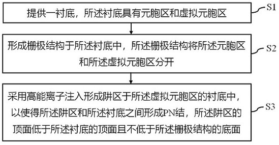
[0047] An embodiment of the present invention provides a method for manufacturing an insulated gate bipolar transistor, see figure 1 , figure 1 It is a flowchart of a method for manufacturing an insulated gate bipolar transistor according to an embodiment of the present invention, and the method for manufacturing an insulated gate bipolar transistor includes:

[0048] Step S1, providing a substrate, the substrate has a cell region and a dummy cell region;

[0049] Step S2, forming a gate structure in the substrate, the gate ...


PUM

PropertyMeasurementUnit
thicknessaaaaaaaaaa
thicknessaaaaaaaaaa
thicknessaaaaaaaaaa

Abstract

The invention provides an insulated gate bipolar transistor and a manufacturing method thereof, and the manufacturing method of the insulated gate bipolar transistor comprises the steps: providing a substrate which is provided with a cell region and a virtual cell region; forming a gate structure in the substrate, wherein the gate structure separates the cell region from the virtual cell region; and forming a well region in the substrate of the virtual cellular region by adopting high-energy ion implantation, so that a PN junction is formed between the well region and the substrate, and the top surface of the well region is lower than the top surface of the substrate and is not lower than the bottom surface of the gate structure. According to the technical scheme, the junction depth of thePN junction in the virtual cellular region can be accurately controlled, so that the withstand voltage of the device is improved, the saturation voltage drop of the device is reduced, and the stability and uniformity of the threshold voltage are improved.

Description

technical field [0001] The invention relates to the technical field of semiconductors, in particular to an insulated gate bipolar transistor and a manufacturing method thereof. Background technique [0002] IGBT (Insulated Gate Bipolar Transistor) is a device composed of MOSFET (input stage) and PNP transistor (output stage). It has the characteristics of easy driving, low input impedance and fast switching speed of MOSFET devices, and Bipolar devices have the advantages of large on-state current density, low on-state voltage, low loss, and good stability. [0003] Among them, the carrier storage trench gate IGBT adopts a dummy cell design when adjusting the saturation voltage drop (VCE(sat)) and switching performance of the device. In the existing virtual cell structure, a P-ring (P-ring) is formed by a combination of ion implantation and thermal diffusion (drive). The specific steps include: first ion implantation on the top surface of the substrate, and then Thermal pro...

Claims


Application Information

Patent Timeline
Patent Type & Authority Applications(China)
IPC IPC(8): H01L29/739H01L21/331H01L29/06
CPCH01L29/0615H01L29/66325H01L29/7393
Inventor 徐旭东王聪梁昕
Owner SEMICON MFG ELECTRONICS (SHAOXING) CORP
Why Eureka
Try Eureka