Circuit for testing output characteristics of a GaN power device

A technology for output characteristics and testing circuits, which is applied in the direction of single semiconductor device testing, measuring electricity, and measuring electrical variables. It can solve problems such as complex operations, time-consuming and labor-consuming, and inaccurate test results, so as to avoid interference and improve accuracy. Effect

Pending Publication Date: 2020-11-17
CHINA EPRI SCIENCE & TECHNOLOGY CO LTD +1
View PDF0 Cites 4 Cited by
  • Summary
  • Abstract
  • Description
  • Claims
  • Application Information

AI Technical Summary

Problems solved by technology

This method is complex to operate, time-consuming and labor-intensive, and has not been studied from the perspective of the application of GaN power devices, resulting in inaccurate test results

Method used


Image

  • Circuit for testing output characteristics of a GaN power device
  • Circuit for testing output characteristics of a GaN power device
  • Circuit for testing output characteristics of a GaN power device

Examples


Embodiment Construction

[0040] The specific embodiments of the present invention will be further described in detail below in conjunction with the accompanying drawings.

[0041] In order to make the objectives, technical solutions, and advantages of the embodiments of the present invention clearer, the technical solutions in the embodiments of the present invention will be described clearly and completely in conjunction with the accompanying drawings in the embodiments of the present invention. Obviously, the described embodiments It is a part of the embodiments of the present invention, not all the embodiments. Based on the embodiments of the present invention, all other embodiments obtained by those of ordinary skill in the art without creative work shall fall within the protection scope of the present invention.

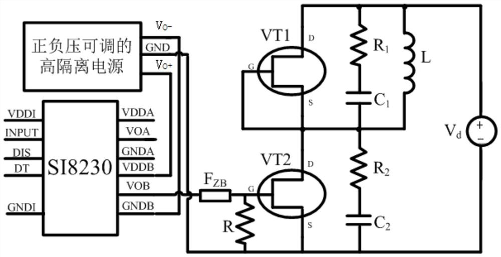
[0042] The invention provides a test circuit for the output characteristics of GaN power devices, such as figure 1 Shown, including:

[0043] Isolated drive chip, GaN power switching device ...


PUM


Abstract

The invention discloses a circuit for testing output characteristics of a GaN power device and a control method. The circuit comprises an isolation driving chip, a GaN power switching device VT1, a first RC absorption protection circuit, an inductor L, a driving magnetic bead FZB, a resistor R, a GaN power switching device VT2 to be tested, a second RC absorption protection circuit, a direct-current power supply Vd and a high-isolation power supply. According to the circuit provided by the invention, the output characteristics of the GaN power device can be tested on a very small tooling plate, electromagnetic interference and parasitic parameters caused by a control signal and a main line connecting line can be effectively avoided, and the accuracy of a test result is improved.

Description

Technical field [0001] The invention relates to the field of power electronics testing, in particular to a test circuit and control method for the output characteristics of a GaN power device. Background technique [0002] The performance of silicon power devices has reached its limit. Compared with traditional silicon power devices, the performance of wide-gap power semiconductors is much better. Among them, the most representative wide-gap power semiconductor device should be gallium nitride power component. Gallium nitride power devices adopt high electron mobility transistor structure, the switching process is very fast, and high frequency switching can be realized. Compared with traditional silicon power devices, under the same withstand voltage, the volume of gallium nitride die is It is much smaller and the parasitic capacitance is small, which helps to increase the switching speed. However, the performance research of gallium nitride power devices is not perfect, and th...

Claims


Application Information

Patent Timeline
Patent Type & Authority Applications(China)
IPC IPC(8): G01R31/26
CPCG01R31/2601G01R31/2607G01R31/2637
Inventor 王蓓蓓栾洪洲朱宁辉张良王轩董亮燕翚刘道民张彬
Owner CHINA EPRI SCIENCE & TECHNOLOGY CO LTD
Why Eureka
Try Eureka