Visible light communication LED array and preparation method thereof

A technology of LED array and visible light communication, applied in electrical components, electric solid devices, circuits, etc., can solve the problems of rising signal-to-noise ratio, restricting the development of VLC technology, unfavorable communication, etc., to improve modulation bandwidth and optical power, improve signal Transmission quality, improved uniformity effect

Pending Publication Date: 2020-11-17
INST OF SEMICONDUCTORS - CHINESE ACAD OF SCI
View PDF0 Cites 1 Cited by
  • Summary
  • Abstract
  • Description
  • Claims
  • Application Information

AI Technical Summary

Problems solved by technology

[0003] Studies have shown that the modulation bandwidth of LED devices plays a decisive role in the modulation bandwidth and transmission speed of visible light communication systems. However, the bandwidth of commercial phosphor-type white light LEDs currently used is generally less than 3MHz, and there is a large distance from the target suitable for communication. , which greatly limits the further development of VLC technology
Although the hot micro-LEDs can obtain high modulation bandwidth by reducing the device size, reducing the RC time constant and increasing the carrier radiation recombination rate, the optical power is often very low due to the sacrifice of the light-emitting area of ​​the active region, while the optical power The reduction of the output will have two effects. On the one hand, it cannot realize its purpose as a lighting source, and on the other hand, it is not conducive to communication, because the small optical power will lead to an increase in the signal-to-noise ratio, which is not conducive to signal transmission.

Method used


Image

  • Visible light communication LED array and preparation method thereof
  • Visible light communication LED array and preparation method thereof
  • Visible light communication LED array and preparation method thereof

Examples


Embodiment Construction

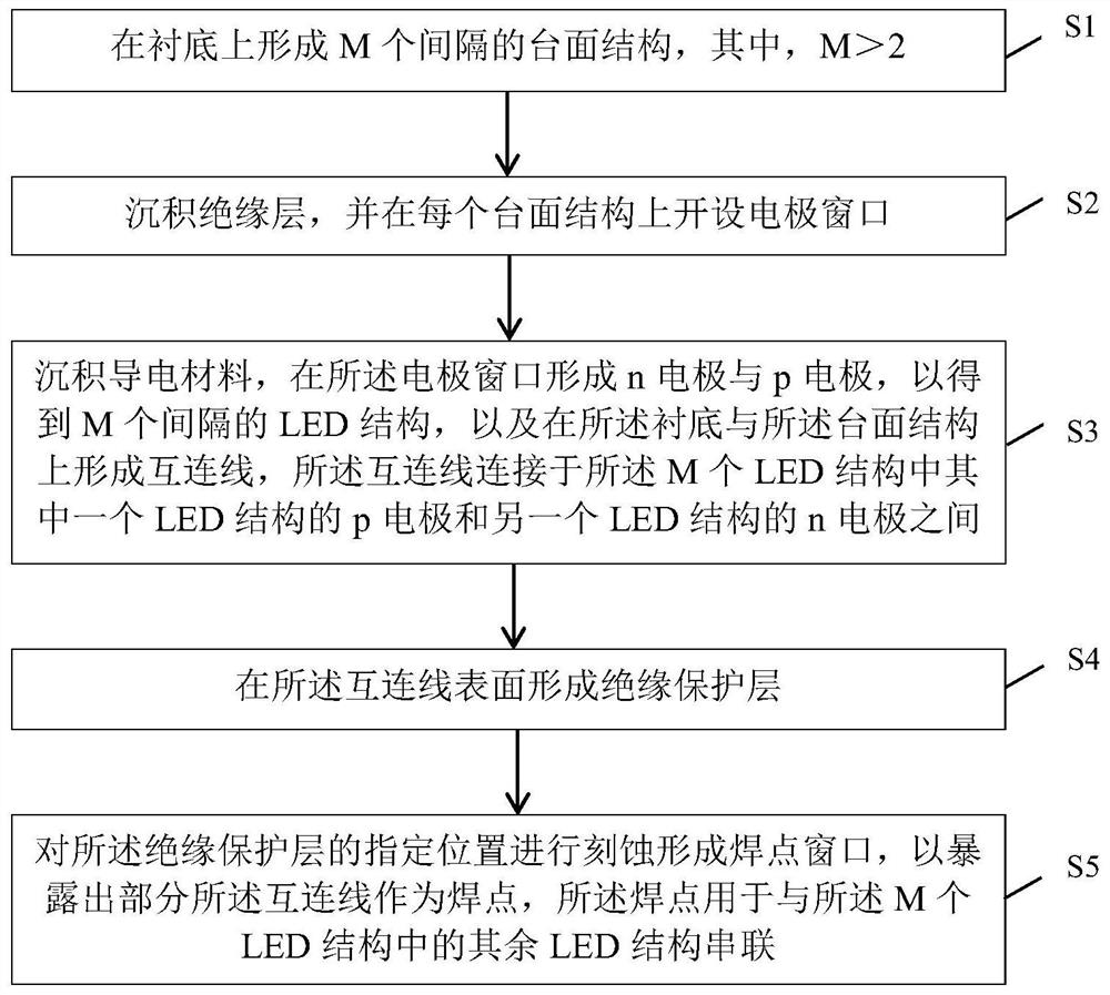
[0039] The technical solution of the present invention will be described in detail below in conjunction with the accompanying drawings and specific embodiments. It should be understood that these embodiments are only used to illustrate the present invention and are not intended to limit the scope of the present invention. After reading the present invention, those skilled in the art Modifications to various equivalent forms of the present invention fall within the scope defined by the appended claims of the present invention.

[0040] Unless otherwise defined, all technical and scientific terms used herein have the same meaning as commonly understood by one of ordinary skill in the technical field of the invention. The terminology used herein in the description of the present invention is only for the purpose of describing specific embodiments, and is not intended to limit the present invention.

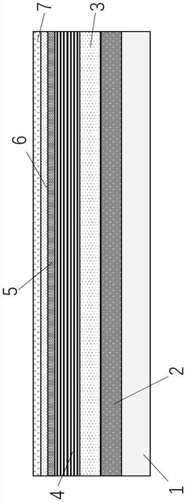
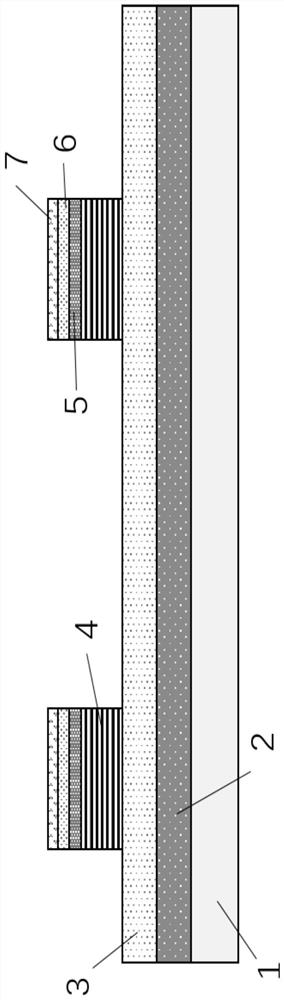
[0041] A visible light communication LED array provided for an embodiment of the...


PUM

PropertyMeasurementUnit
sizeaaaaaaaaaa
thicknessaaaaaaaaaa
thicknessaaaaaaaaaa

Abstract

The invention provides a visible light communication LED array and a preparation method thereof. The visible light communication LED array comprises a substrate, wherein the M LED structures are located on the substrate at intervals, M is larger than 2, and each LED structure comprises a mesa structure, an n electrode and a p electrode, and the n electrode and the p electrode are located on the mesa structure; an interconnection line located on the substrate and the mesa structure, wherein the interconnection line is connected between the p electrode of one LED structure and the n electrode ofthe other LED structure in the M LED structures; an insulating protection layer positioned on the interconnection line; and a welding spot window penetrating through the insulating protective layer so as to expose part of the interconnection line as a welding spot, wherein the welding spot is connected with the LED structure in series. The visible light communication LED array provided by the invention can improve the modulation bandwidth and the optical power at the same time, thereby improving the signal transmission quality in visible light communication.

Description

technical field [0001] The invention relates to the field of semiconductors, in particular to a visible light communication LED array and a preparation method thereof. Background technique [0002] In recent years, smart products such as smart homes and smart bracelets have become popular, and new interactive controls have brought unprecedented challenges to traditional network access technologies. The above problems all require a mobile access method that can broaden spectrum resources and it is against this background that visible light communication (Visible Light Communication, VLC) emerged. Visible light communication uses white light LED as a light source to achieve high-speed communication while illuminating. Compared with traditional light sources, LED not only has the advantages of low energy consumption, environmental friendliness, and reliable life, but also has higher modulation bandwidth and corresponding sensitivity. Taking advantage of these characteristics,...

Claims


Application Information

Patent Timeline
Patent Type & Authority Applications(China)
IPC IPC(8): H01L27/15H01L33/38H01L33/62
CPCH01L27/156H01L33/38H01L33/62H01L2933/0016H01L2933/0066
Inventor 赵丽霞林杉
Owner INST OF SEMICONDUCTORS - CHINESE ACAD OF SCI
Why Eureka
Try Eureka