
Super junction semiconductor device and manufacturing method of super junction semiconductor device

一种超结半导体、制造方法的技术,应用在半导体/固态器件制造、半导体器件、电气元件等方向,能够解决耐压降低、提高、通态电阻增加等问题,达到抑制雪崩耐量降低的效果

Pending Publication Date: 2020-11-17
FUJI ELECTRIC CO LTD
View PDF1 Cites 1 Cited by
  • Summary
  • Abstract
  • Description
  • Claims
  • Application Information

AI Technical Summary

Problems solved by technology

Therefore, the maximum electric field strength is reached immediately and the withstand voltage is reduced
On the other hand, in order to increase the withstand voltage of the vertical MOSFET, it is necessary to increase the thickness of the n-type drift layer, but the on-state resistance increases
Such a relationship between on-state resistance and withstand voltage is called a trade-off relationship, and it is usually difficult to improve both parties in the trade-off relationship.

Method used


Image

  • Super junction semiconductor device and manufacturing method of super junction semiconductor device
  • Super junction semiconductor device and manufacturing method of super junction semiconductor device
  • Super junction semiconductor device and manufacturing method of super junction semiconductor device

Examples


Embodiment approach

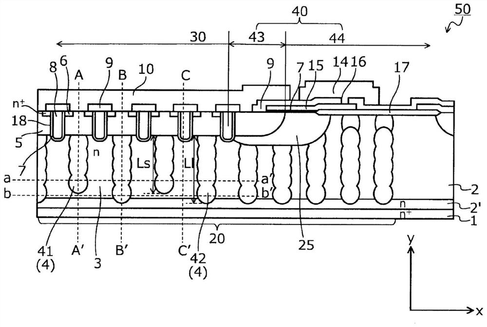
[0099] The super junction semiconductor device of the present invention will be described by taking the SJ-MOSFET as an example. figure 1 is a cross-sectional view showing the structure of the SJ-MOSFET of the embodiment.

[0100] figure 1 The shown SJ-MOSFET 50 is equipped with a MOS (Metal Oxide Semiconductor: Metal Oxide Semiconductor) on the front side (the surface on the side of the p-type base region 5 described later) of a semiconductor substrate (silicon substrate: semiconductor chip) containing silicon (Si). ) gate of the SJ-MOSFET50. This SJ-MOSFET 50 includes an active region 30 and an edge termination region 40 surrounding the active region 30 . The active region 30 is a region where current flows in the on state. The edge termination region 40 includes a withstand voltage holding region 44 that relaxes the electric field on the front side of the semiconductor body in the drift region and maintains a withstand voltage, and a boundary region 43 between the with...


PUM


Abstract

The invention provides a super-junction semiconductor device and a method of manufacturing the super-junction semiconductor device capable of suppressing a decrease in avalanche tolerance even in a state where a charge balance is "1". The semiconductor device includes an active region (30) through which a current flows, and a terminal structure portion (40). A first semiconductor layer (2) of a first conductivity type is provided on the front surface of a semiconductor substrate (1) of the first conductivity type. The surface of the first semiconductor layer (2) is provided with a parallel p-nstructure (20) in which first columns (3) of the first conductivity type and second columns (4) of the second conductivity type are repeatedly and alternately arranged on a surface parallel to the front surface. The second pillar (4) of the active region (30) includes a first region (41) in which the distance between the bottom surface of the second pillar (4) and the front surface of the semiconductor substrate (1) is longer than the distance between the bottom surface of the second pillar (4) and the front surface of the semiconductor substrate (1) in the second region (42).

Description

technical field [0001] The invention relates to a super junction semiconductor device and a method for manufacturing the super junction semiconductor device. Background technique [0002] In a normal n-channel vertical MOSFET (Metal Oxide Semiconductor Field Effect Transistor: Insulated Gate Field Effect Transistor), the n-type drift layer is the semiconductor layer with the highest resistance among the plurality of semiconductor layers formed in the semiconductor substrate. The resistance of this n-type drift layer greatly affects the on-state resistance of the entire vertical MOSFET. The overall on-resistance of the vertical MOSFET can be reduced by reducing the thickness of the n-type drift layer and shortening the current path. [0003] However, the vertical MOSFET also has a function of maintaining a withstand voltage by extending the depletion layer to the high-resistance n-type drift layer in the off state. Therefore, in the case of thinning the n-type drift layer i...

Claims


Application Information

Patent Timeline
Patent Type & Authority Applications(China)
IPC IPC(8): H01L29/06H01L29/78H01L21/336
CPCH01L29/0615H01L29/0603H01L29/0684H01L29/78H01L29/66477H01L29/0696H01L29/7397H01L29/0619H01L29/66348H01L29/0634H01L29/7813H01L29/7811H01L29/66734H01L29/0638H01L29/7802H01L29/66712H01L29/1095
Inventor 西村武义前田凉菅井勇
Owner FUJI ELECTRIC CO LTD
Features
  • Generate Ideas
  • Intellectual Property
  • Life Sciences
  • Materials
  • Tech Scout
  • Unparalleled Data Quality
  • Higher Quality Content
  • 60% Fewer Hallucinations
Learn More