
A product surface defect detection method, system, device and medium

A defect detection and product technology, applied in neural learning methods, image analysis, image enhancement, etc., can solve problems such as high time cost and labor cost, slow algorithm update, difficulty adapting to new product pictures, etc., to save manpower input and avoid Effects of Dependency, Fast Convergence Speed, and Refactoring Quality

Active Publication Date: 2022-08-02
CHENGDU UNION BIG DATA TECH CO LTD
View PDF16 Cites 0 Cited by
  • Summary
  • Abstract
  • Description
  • Claims
  • Application Information

AI Technical Summary

Problems solved by technology

This type of method mainly faces four problems in practical application. First, it needs to collect a large number of defect pictures as training data. The collection of low-probability defect pictures in actual production requires high time and labor costs; second, based on the existing The automatic surface defect detection algorithm for training pictures cannot cope with the unknown defect manifestations that may occur in production. The method based on supervised learning can achieve a better generalization effect on the defect forms contained in the training data set, while the actual production The sudden unknown new defects in the process do not exist in the existing training pictures, and the algorithm may miss detection of defects, resulting in production losses; third, a large number of manually labeled defect pictures, object detection and semantic segmentation, etc. The cost is high and the time required is long, which leads to the slow response of the algorithm to changes in production conditions and poor timeliness; fourth, it is difficult to adapt to new product pictures. In supervised learning, good product pictures without defects are used as negative For learning from pictures, the background of new product pictures that do not exist in the training data may change greatly, which may cause the algorithm to over-check the defects. To solve this problem, it is necessary to invest in manpower to collect and label new product pictures in time , and then optimize the model, resulting in slower algorithm update

Method used


Image

  • A product surface defect detection method, system, device and medium
  • A product surface defect detection method, system, device and medium

Examples


Embodiment 1

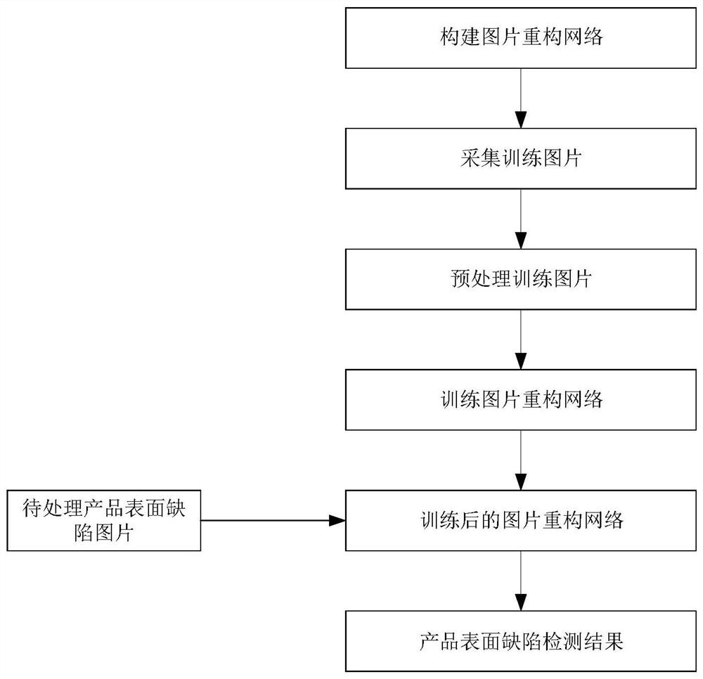
[0044] Embodiment 1 of the present invention provides a method for detecting surface defects of products. Please participate in figure 1 , figure 1 It is a schematic flow chart of a product surface defect detection method, the method includes:

[0045] Step 1: Design the structure of a deep convolutional neural network based on a fully convolutional network. The process of the network processing images mainly includes: a downsampling process, an upsampling process and a cross-layer linking process. The downsampling process includes: multi-layer 3*3 convolution, batch normalize and relu activation function. The upsampling process includes 2-fold upsampling, i.e. using interpolation algorithm to double the input feature map size, convolutional layers, batch normalization and relu activation function. Several feature maps in the downsampling process are directly added to the feature maps of the corresponding scale in the upsampling process, forming a cross-layer linking process...

Embodiment 2

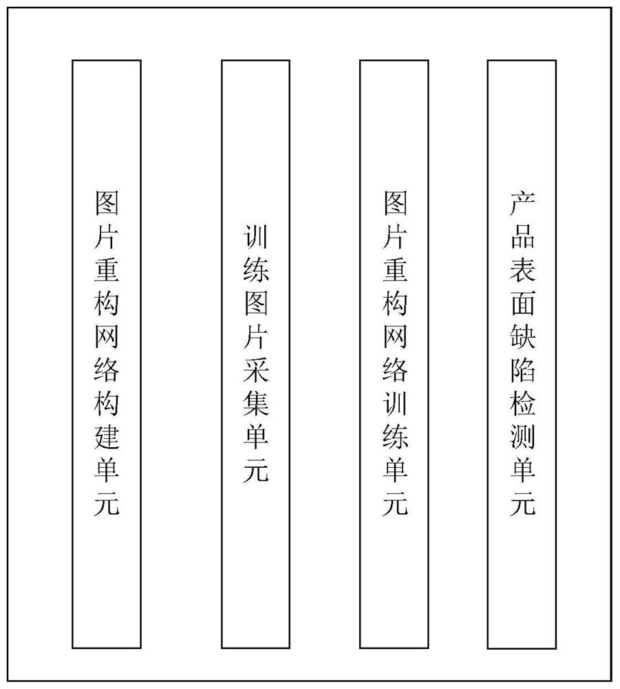
[0054] The second embodiment of the present invention provides a product surface defect detection system, the system includes:

[0055] The image reconstruction network construction unit is used to construct an image reconstruction network. The processing process of the image by the image reconstruction network includes: a downsampling process, an upsampling process and a cross-layer linking process; the downsampling process includes: the image is processed by the convolution layer , and then perform batch normalization processing, and then use the activation function to activate; the upsampling process includes: the image is processed by the convolution layer, then batch normalized, and then activated using the activation function; the cross-layer linking process includes: Several feature maps in the downsampling process are added to the feature maps of the corresponding scale in the upsampling process;

[0056] The training picture collection unit is used to collect defect-f...

Embodiment 3

[0060] Embodiment 3 of the present invention provides a product surface defect detection device, including a memory, a processor, and a computer program stored in the memory and executable on the processor, when the processor executes the computer program The steps of implementing the method for detecting surface defects of a product.


PUM


Abstract

The invention discloses a product surface defect detection method, system, device and medium, comprising: constructing a picture reconstruction network; collecting training pictures for a defect-free picture method; using the training pictures to train the picture reconstruction network to obtain the trained picture reconstruction network; collect pictures of surface defects of products to be processed, input the pictures of surface defects of products to be processed into the image reconstruction network after training, calculate the eigenvalues ​​of pictures of surface defects of products to be processed and reconstructed pictures, and calculate surface defects of products to be processed The difference between the eigenvalues ​​of the picture and the reconstructed picture, the product surface defect detection result is obtained based on the difference of the eigenvalues; the present invention only uses the good picture for surface defect detection, and the present invention is based on the full convolutional neural network, by reconstructing the good picture. Learn the ability to repair surface defects, so as to achieve pixel-level recognition capabilities for various surface defects.

Description

technical field [0001] The invention relates to the technical field of intelligent manufacturing and artificial intelligence, and in particular, to a method, system, device and medium for detecting surface defects of products. Background technique [0002] Surface defect detection algorithms based on machine vision mainly include traditional vision methods and deep learning methods. Traditional visual methods are mainly based on artificially designed visual features, such as watershed algorithm, LBP feature method, etc., while deep learning methods are mainly based on convolutional neural networks, such as Faster RCNN algorithm, MASK RCNN algorithm, etc. The use of deep learning methods in automatic surface defect detection algorithms is currently gaining popularity. [0003] In the current surface defect detection methods using deep learning, supervised learning methods such as target detection algorithms or semantic segmentation algorithms are mainly used. This type of m...

Claims


Application Information

Patent Timeline
Patent Type & Authority Patents(China)
IPC IPC(8): G06T7/00G06N3/08G06N3/04G06T7/174G06T5/00
CPCG06T7/0004G06N3/08G06T7/174G06T5/005G06T2207/20084G06T2207/20081G06T2207/30161G06T2207/30136G06T2207/30124G06N3/045
Inventor 不公告发明人
Owner CHENGDU UNION BIG DATA TECH CO LTD
Learn More