High-density small-spacing LED module with graphic hollow interlayer, display and method

A LED module and small-pitch technology, applied in static indicators, instruments, electric solid devices, etc., can solve the problems of easy crushing of metal pillars, too small bonding area, insufficient bonding strength, etc., to improve light output Efficiency, increased bonding area, and increased bonding strength

Active Publication Date: 2020-11-20
JIHUA LAB
View PDF6 Cites 0 Cited by
  • Summary
  • Abstract
  • Description
  • Claims
  • Application Information

AI Technical Summary

Problems solved by technology

[0007] The purpose of the present invention is to provide a high-density small-pitch LED module, display and method with a hollowed-out interlayer, aiming at solving the problem that the existing high-density small-pitch LED display unit structure based on a glass substrate adopts a connection method of metal pillars. Too small bonding area leads to insufficient bonding strength and the problem that the metal pillar is easily broken during use

Method used


Image

  • High-density small-spacing LED module with graphic hollow interlayer, display and method
  • High-density small-spacing LED module with graphic hollow interlayer, display and method
  • High-density small-spacing LED module with graphic hollow interlayer, display and method

Examples


preparation example Construction

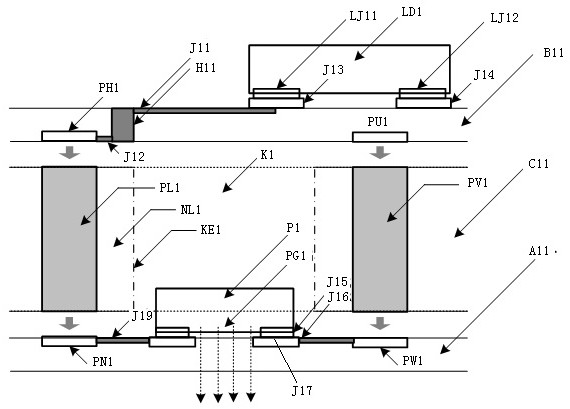
[0061] like Figure 5 As shown in the above, a method for preparing a high-density small-pitch LED module with a pattern hollowed out and connected with a sandwich layer as described above specifically includes the following steps:

[0062] S1: prepare a glass carrier, and mount the LED flip-chip light-emitting chip on the glass carrier;

[0063] S2: prepare a driver carrier board, and install the driver chip on the driver carrier board;

[0064] S3: Prepare a patterned hollow interconnection interlayer, set according to the position where the LED flip-chip light-emitting chip is mounted on the glass carrier, the position where the driver chip is mounted on the driver carrier, and the connection position relationship between the LED flip-chip light-emitting chip and the driver chip The conductive material part, the patterned hollow part and the non-conductive material part make the LED flip-chip light-emitting chip wrapped in the patterned hollow part, and the LED flip-chip l...

Embodiment 1

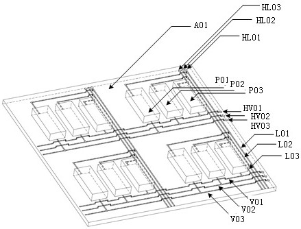
[0071] This embodiment is the production process of the high-density small-pitch LED display unit module based on the patterned hollowing and pressing of the Unicom interlayer, as shown in the appendix. Figure 6a As shown in the figure, it includes a component with a glass carrier as the main body and a component with a printed circuit carrier as the main body; A21 in the figure is a glass carrier, P21, P22, P23 are respectively the reverse side light-emitting red primary color LED flip-chip light-emitting chip, the reverse side The light-emitting green primary color LED flip-chip structure light-emitting chip and the reverse light-emitting blue primary color LED flip-chip structure light-emitting chip (see attached Figure 6a The dashed line on the back of the glass carrier A1), the light-emitting surface of the LED flip-chip light-emitting chip is on the upper part of the glass carrier A21 (as indicated by the dashed arrow); V21, V22, V23 are red, green, and blue LEDs Displ...

Embodiment 2

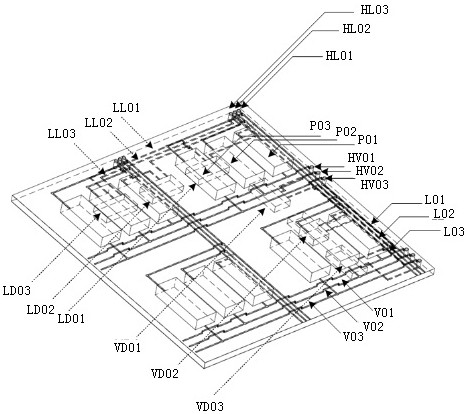
[0074] This embodiment is the production process of generating high-density small-pitch LED display unit modules based on patterned hollowing and pressing the interconnected interlayer (that is, when the patterned hollowing part is set to a large hollow space), as shown in the appendix. Figure 7a As shown, it includes a component with a glass carrier as the main body and a component with a printed circuit carrier as the main body; A31 is the glass carrier in the figure, P31, P32, P33 are the reverse light-emitting red primary color LED flip-chip structure light-emitting chip, the reverse side The light-emitting green primary color LED flip-chip structure light-emitting chip and the reverse light-emitting blue primary color LED flip-chip structure light-emitting chip (see attached Figure 7aThe dashed line on the back of the middle glass carrier A31), the light-emitting surface of the LED flip-chip light-emitting chip is on the upper part of the glass carrier A31 (as shown by t...


PUM


Abstract

The invention discloses a high-density small-spacing LED module with a graphic hollow interlayer, a display and a method. The graphical hollowed-out part is arranged to be communicated with the interlayer; other parts, except the conductive material part and the graphical hollow part, in the graphical hollow communicating interlayer are filled with a non-conductive material part; the bonding areaof the whole structure is greatly increased, so that the bonding strength is improved; the problem that the conductive material part is broken by pressing in the use process is solved; the conductivematerial part is not changed; therefore, the connection conductive effect of the light-emitting chip and the driving chip of the LED flip structure and the light-emitting effect of the whole high-density small-spacing LED module can be ensured. And moreover, the processing technology of the whole high-density small-spacing LED module is relatively simple, and other use and production requirementsare met at the same time on the premise of meeting bonding and compressive strength.

Description

technical field [0001] The invention relates to the technical fields of high-density LED display and semiconductor materials, and in particular to a high-density small-pitch LED module, display and method with a pattern hollow sandwich. Background technique [0002] At present, high-density small-pitch LED display products, especially COB high-density LED display, are directly assembled with small-sized LED chips and PCB boards for ultra-high precision. The overall potting protection solves the problems of ultra-high-density component layout and wiring and high reliability, and the high-precision assembly of the array module and display unit realizes the LED large-screen splicing display. [0003] figure 1 In order to use the LED flip-chip structure light-emitting chip high-density COB package display array module to enlarge the surface schematic diagram, the structure is explained on this drawing: A01 is the high-density COB package display array module carrier board, and ...

Claims


Application Information

Patent Timeline
Patent Type & Authority Applications(China)
IPC IPC(8): H01L33/48H01L33/62H01L25/16G09G3/32
CPCG09G3/32H01L25/165H01L25/167H01L33/486H01L33/62H01L2933/0033H01L2933/0066
Inventor 郑喜凤王瑞光陈宇汪洋王铂
Owner JIHUA LAB
Why Eureka
Try Eureka