
Semiconductor chip dehumidification method

A semiconductor and chip technology, applied in the direction of drying solid materials, drying gas arrangement, drying solid materials without heating, etc., can solve the problems of affecting the process, inability to dry, poor dehumidification and drying effect, etc., and achieve the effect of ensuring high efficiency

Inactive Publication Date: 2020-11-27
涌明科技(上海)有限公司
View PDF10 Cites 0 Cited by
  • Summary
  • Abstract
  • Description
  • Claims
  • Application Information

AI Technical Summary

Problems solved by technology

[0003] The existing semiconductor chips need to be cleaned during the production and processing process. After cleaning, they need to be dried and dehumidified. Therefore, a dehumidification device is required to use the existing dehumidification method for dehumidification. However, the existing dehumidification method is relatively simple, just using a fan Air-dry the chips conveyed on the surface of the conveyor belt, but the surface in contact with the conveyor belt cannot be dried, and the dehumidification and drying effect is not good, and the dehumidification is not complete, which affects the subsequent process

Method used


Image

  • Semiconductor chip dehumidification method
  • Semiconductor chip dehumidification method

Examples


Embodiment Construction

[0025] The following will clearly and completely describe the technical solutions in the embodiments of the present invention with reference to the accompanying drawings in the embodiments of the present invention. Obviously, the described embodiments are only some, not all, embodiments of the present invention.

[0026] In describing the present invention, it should be understood that the terms "upper", "lower", "front", "rear", "left", "right", "top", "bottom", "inner", " The orientation or positional relationship indicated by "outside", etc. is based on the orientation or positional relationship shown in the drawings, and is only for the convenience of describing the present invention and simplifying the description, rather than indicating or implying that the referred device or element must have a specific orientation, so as to Specific orientation configurations and operations, therefore, are not to be construed as limitations on the invention.

[0027] In the description...


PUM


Abstract

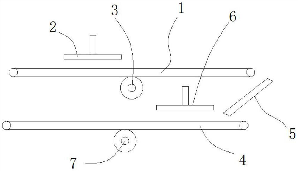
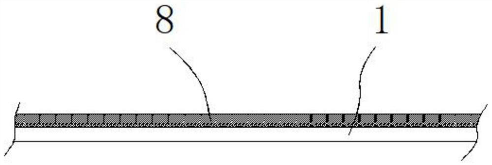
The invention belongs to the field of semiconductor chip processing, and particularly relates to a semiconductor chip dehumidification method. A dehumidification system used in the dehumidification method comprises a first conveyor belt, a first fan, a second conveyor belt and a second fan, wherein the first fan is mounted on the upper side of the surface of the first conveying belt, and an air outlet of the first fan directly faces the upper surface of the first conveying belt. According to the method, when a single surface of a chip is air-dried and dehumidified through the fan, a water absorption cotton layer on the surface of the first conveying belt can absorb water molecules on the other surface of the chip, and then the surface of the semiconductor chip is air-dried and moisture-absorbed again through a guide plate, so that the semiconductor chip can be thoroughly dried, therefore, the situation that the subsequent process is influenced by incomplete dehumidification is effectively avoided.

Description

technical field [0001] The invention relates to the field of semiconductor chip processing, in particular to a semiconductor chip dehumidification method. Background technique [0002] Semiconductor chip: A semiconductor device that can realize a certain function is made by etching and wiring on a semiconductor sheet. Not only silicon chips, but also gallium arsenide (gallium arsenide is poisonous, so some inferior circuit boards should not be curious to decompose it), germanium and other semiconductor materials. Semiconductors are also trendy like cars. In the 1970s, American companies such as Intel had the upper hand in the dynamic random access memory (D-RAM) market. However, in the 1980s when high-performance D-RAM was required due to the emergence of large-scale computers, Japanese companies came out on top. [0003] The existing semiconductor chips need to be cleaned during the production and processing process. After cleaning, they need to be dried and dehumidified...

Claims


Application Information

Patent Timeline
Patent Type & Authority Applications(China)
IPC IPC(8): F26B17/04F26B5/16F26B21/00F26B23/00
CPCF26B5/16F26B17/04F26B21/004F26B23/00
Inventor 李双玉
Owner 涌明科技(上海)有限公司
Learn More