Supercharge Your Innovation With Domain-Expert AI Agents!

Voltage-drop-circuit-based MOS transistor verification fixing architecture and verification method

A MOS tube and circuit technology, applied in the field of MOS tube verification and verification based on voltage drop circuits, can solve the problems of misjudgment, waste of space, and overall design exceeding specifications by designers and verifiers, so as to reduce considerations and costs. , Wide application prospect, reliable effect of design principle

Active Publication Date: 2020-11-27
INSPUR SUZHOU INTELLIGENT TECH CO LTD
View PDF5 Cites 0 Cited by
  • Summary
  • Abstract
  • Description
  • Claims
  • Application Information

AI Technical Summary

Problems solved by technology

But in practice, the instability of the test points selected when verifying the design circuit causes the resonance of the voltage waveform, which makes the actual value deviate from the verified value, causing misjudgment by designers and verifiers, so that the overall design exceeds specs, waste of space
[0004] At present, there is no perfect solution to the above problems. The usual method is to only shorten the extension line of the test point, or increase the buffer, and gradually reduce the voltage waveform Resonance, but these two methods will reduce the efficiency of the overall step-down converter; among them, shortening the extension line of the test point will increase the doubt that the extension line of the test point will short circuit with other credit lines or power lines, and increase the tinning The difficulty of the overall verification will increase relatively; the verification method is not fixed and the judgment of the verification report will be seriously affected. If there is no way to distinguish the misjudgment, it is necessary to increase the buffer or copper to solve the misjudgment problem, but in this way It will bring additional problems such as reducing the overall efficiency of the step-down converter, generating heat, and increasing production costs, and the desired effect cannot be achieved.

Method used


Image

  • Voltage-drop-circuit-based MOS transistor verification fixing architecture and verification method

Examples


Embodiment 1

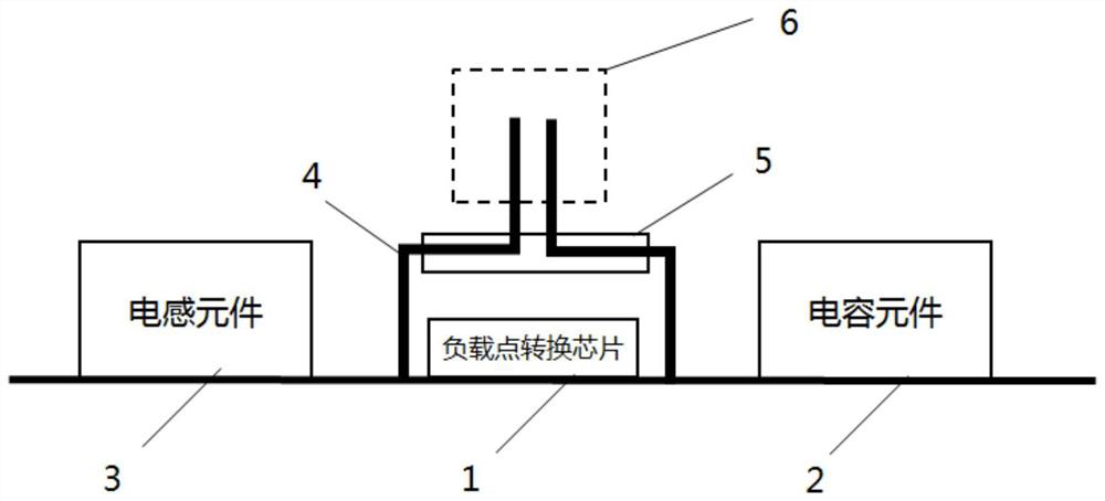
[0026] Such as figure 1 As shown, this embodiment provides a MOS transistor verification and fixed architecture based on a voltage drop circuit, including: the voltage drop circuit includes: a point-of-load conversion chip 1, a capacitive element 2, and an inductive element 3, and the point-of-load conversion chip 1, a frame 4 and an insulating plate 5 are arranged above, and the insulating plate 5 is embedded in the top of the frame 4. The frame 4 includes two low-impedance and high-conduction rods, and the bottom ends of the two low-impedance and high-conduction rods are connected to the capacitive element 2 respectively. , the inductance element 3 is connected, and the tops of the two low-impedance and high-conduction bars constitute the test point 6 for MOS tube verification; the insulating plate is an insulating plastic plate, and the size of the insulating plate is larger than the point-of-load conversion chip; The above architecture is set on the power board by means of...


PUM


Abstract

The invention provides a voltage-drop-circuit-based MOS transistor verification fixing architecture and a verification method. The voltage-drop-circuit-based MOS transistor verification fixing architecture comprises a voltage drop circuit including a load point conversion chip, a capacitance element and an inductance element; a frame and an insulating plate are arranged above the load point conversion chip, the insulating plate is embedded into the top of the frame, the frame comprises two low-impedance high-conduction rods, the bottom ends of the two low-impedance high-conduction rods are respectively connected with the capacitance element and the inductance element, and the top ends of the two low-impedance high-conduction rods form a test point for MOS tube verification. By arranging the fixing frame, verification errors, caused by instability of test points, of the MOS tubes are reduced, the time needed by misjudgment and debugging after verification testing is effectively shortened, and consideration and cost of adding components are further reduced.

Description

technical field [0001] The invention belongs to the technical field of power supply production inspection, and in particular relates to a voltage-drop circuit-based MOS tube verification fixed structure and verification method. Background technique [0002] Nowadays, POL ("Point of Load", point-of-load converter) has been integrated into the IC chip. Usually, the POL IC chip includes: controller, drive circuit and Power MOSFET. On the actual board side, the POL IC chip is in the voltage drop circuit. Typically designed between MLCCs ("Chip Multilayer Ceramic Capacitors") and Indoctors ("Inductors"). [0003] Based on the actual application of the board and the relationship between the MOSFET manufacturing technology, when designing a step-down switching circuit, there is a certain limit to the difference between the withstand voltage value between the D pole and the S pole of the MOSFET and the voltage value of the input power supply. , Generally, in the selection of the MO...

Claims


Application Information

Patent Timeline
Patent Type & Authority Applications(China)
IPC IPC(8): G01R31/26G01R1/04
CPCG01R31/2621G01R1/0416
Inventor 林鼎焜
Owner INSPUR SUZHOU INTELLIGENT TECH CO LTD
Features
  • R&D
  • Intellectual Property
  • Life Sciences
  • Materials
  • Tech Scout
  • Unparalleled Data Quality
  • Higher Quality Content
  • 60% Fewer Hallucinations
Learn More