Aging clamp for semiconductor laser chip

A technology of lasers and semiconductors, applied in semiconductor lasers, lasers, laser components, etc., can solve the problems of low aging efficiency and achieve the effects of saving time, improving heat dissipation efficiency, and improving work efficiency

Pending Publication Date: 2020-11-27
潍坊华光光电子有限公司
View PDF6 Cites 8 Cited by
  • Summary
  • Abstract
  • Description
  • Claims
  • Application Information

AI Technical Summary

Problems solved by technology

This patent application can only install one laser at a time, and one fixture will age one laser, and the aging efficiency is low

Method used


Image

  • Aging clamp for semiconductor laser chip
  • Aging clamp for semiconductor laser chip
  • Aging clamp for semiconductor laser chip

Examples


Embodiment 1

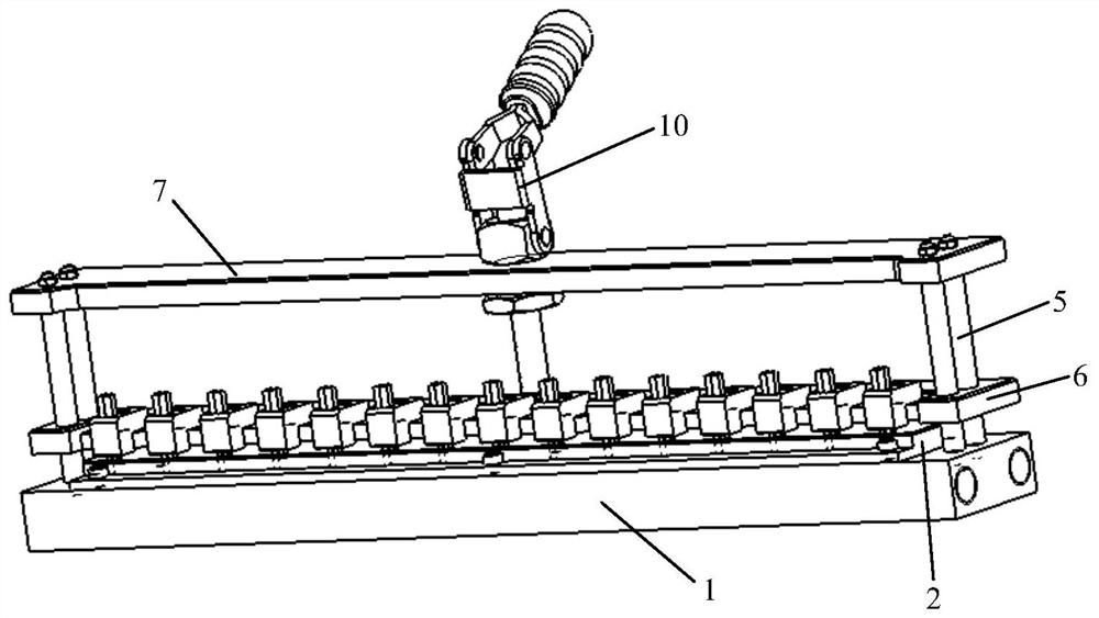
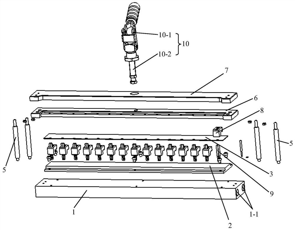
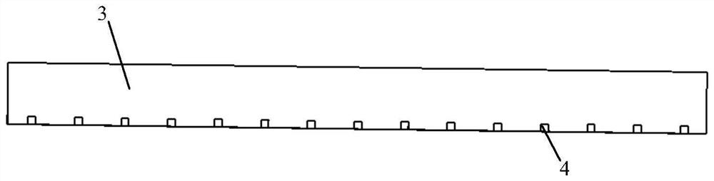
[0036] A kind of aging fixture of semiconductor laser chip, such as Figure 1~6 As shown, it includes the water cooling plate 1, the water cooling plate 1 is a rectangular parallelepiped structure, the upper surface of the water cooling plate 1 is fixed with a COS aging connecting plate 2, the middle part of the COS aging connecting plate 2 is raised, and its cross section is a “convex” shaped structure, and the protrusion is fixed on the There is a circuit board 3, and one side of the circuit board 3 is uniformly provided with a plurality of limiting grooves 4 for placing chips, such as image 3 As shown, the number of limiting slots 4 in this embodiment is 15, and 15 chips can be placed. The circuit board 3 here can connect 15 chips in series for aging, and there is no need to weld densely packed electric wires on the upper end, saving plenty of time;

[0037] Two ends of the water-cooled plate 1 are vertically fixed with a plurality of guide shafts 5, the guide shaft 5 is ...

Embodiment 2

[0041] A kind of burn-in fixture of semiconductor laser chip, its structure is as shown in embodiment 1, and difference is, the side that circuit board 3 is provided with limit groove is aligned with the raised side of COS burn-in joint board 2, namely chip and One side of the bump on the COS burn-in board is aligned, and the chip has an angle when emitting light. The bump is to prevent the light path from hitting the COS burn-in board, which will affect the burn-in effect.

Embodiment 3

[0043]An aging jig for a semiconductor laser chip, its structure is as shown in Embodiment 1, the difference is that the upper surface of the water cooling plate 1 is provided with screw holes for fixed connection with the COS aging connecting plate 2 and the guide shaft 5, all through screw connection, the inside of the water cooling plate 1 is provided with a circulating water channel 1-1 along its length direction, such as figure 2 As shown, the area of ​​the circulating water channel can be maximized, that is, it can occupy the inner space of the water-cooled plate to the maximum, which is beneficial to the heat dissipation of the semiconductor laser, and the heat is taken away by the circulating water in the circulating water channel, saving the aging time. Improved work efficiency.


PUM


Abstract

The invention relates to an aging clamp of a semiconductor laser chip and belongs to the semiconductor aging clamp field. The aging clamp comprises a water cooling plate being of a cuboid structure, aCOS aging connection plate is fixed on the upper surface of the water cooling plate, the middle of the COS aging connection plate is protruded, a circuit board is fixed on the protrusion, and a plurality of limiting grooves used for placing chips are evenly arranged on one side of the circuit board. A plurality of guide shafts are vertically and fixedly arranged at the two ends of the water cooling plate and sleeved with pressing blocks, the pressing blocks can move up and down along the guide shafts, and clamp fixing plates are fixed to the upper ends of the guide shafts; a plurality of probe seats are fixed on the pressing blocks, and probes for pressing the chip are arranged on the probe seats; clamps are arranged on the clamp fixing plates and comprise clamp bodies and telescopic arms, the clamp bodies are fixed to the clamp fixing plates, and one ends of the telescopic arms are connected with the pressing blocks. During aging, rapid and accurate assembly can be achieved, and theworking efficiency is improved.

Description

technical field [0001] The invention relates to an aging fixture for semiconductor laser chips, belonging to the technical field of semiconductor aging fixtures. Background technique [0002] Due to the advantages of small size, light weight, high conversion efficiency and long service life, semiconductor lasers are widely used in medical, display, pumping, industrial processing and other fields. In recent years, with the rapid development of semiconductor material epitaxial growth technology, semiconductor laser waveguide structure optimization technology, cavity surface passivation technology, high stability packaging technology, and efficient heat dissipation technology, especially in the direct semiconductor laser industrial processing applications and high-power optical fiber Driven by the demand for laser pumping, semiconductor lasers with high power and high beam quality have developed rapidly, providing a light source basis for high-quality, high-performance direct s...

Claims


Application Information

Patent Timeline
Patent Type & Authority Applications(China)
IPC IPC(8): G01R31/28G01R1/04H01S5/00H01S5/024
CPCG01R31/2894G01R1/0408H01S5/0021H01S5/02423
Inventor 邵长国马崇彩孙素娟开北超
Owner 潍坊华光光电子有限公司
Why Eureka
Try Eureka