Novel PCB base material structure and PCB lamination manufacturing method using same

A manufacturing method and base material technology, applied in the direction of multilayer circuit manufacturing, printed circuit manufacturing, printed circuit components, etc., can solve problems affecting the conduction of different layers of lines, so as to avoid the problem of unqualified quality, save labor costs, Facilitate the effect of automation

Pending Publication Date: 2020-12-04
PLOTECH TECH KUNSHAN CO LTD
View PDF0 Cites 1 Cited by
  • Summary
  • Abstract
  • Description
  • Claims
  • Application Information

AI Technical Summary

Problems solved by technology

Among them, the alignment of multiple layers is a difficult point, because the conductive lines are getting finer and finer, but the deformation during processing will affect the conduction of different layers of lines

Method used


Image

  • Novel PCB base material structure and PCB lamination manufacturing method using same
  • Novel PCB base material structure and PCB lamination manufacturing method using same
  • Novel PCB base material structure and PCB lamination manufacturing method using same

Examples


Embodiment

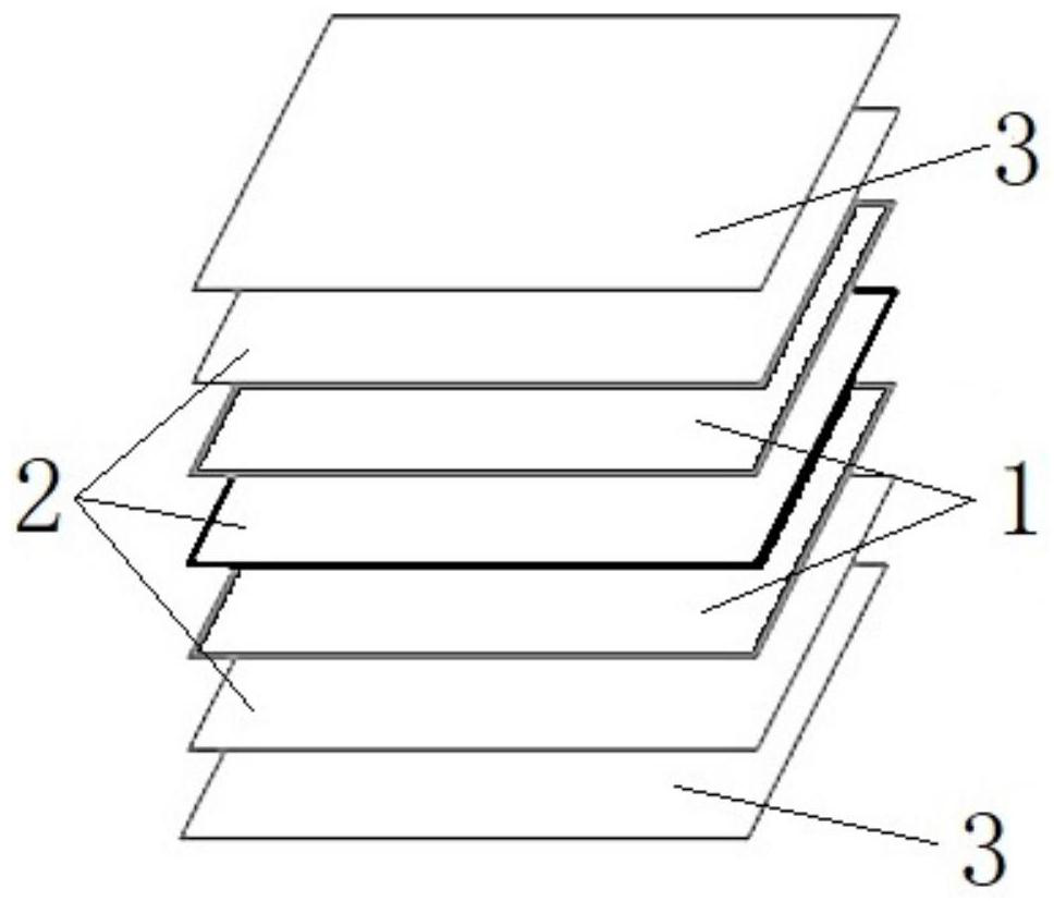
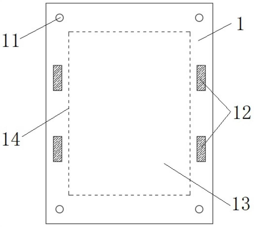
[0033] Such as figure 2 As shown, a novel PCB base material structure of the present invention includes a rectangular base material, and the base material has a circuit part 13 in the middle and several alignment holes 11 located outside the circuit part 13, and the base material 1 is in Fusion blocks 12 are also provided on the outer edge of the line portion 13 . The fusion block 12 is a structure that can be thermally fused, which can combine the edge of the base material 1 with the edge of the dielectric layer 2 to resist deformation during processing.

[0034] At least two fusion blocks 12 are provided on the edge of each long side of the substrate 1 . Because the middle part of the long side is easier to shrink, it is necessary to use multiple fusion blocks 12 to increase the fixed position to further ensure the quality of PCB products.

[0035] Such as Figure 1 to Figure 3 As shown, a novel PCB lamination manufacturing method, the steps include:

[0036] ①Pre-proce...


PUM


Abstract

The invention belongs to the technical field of printed circuit board manufacturing, and relates to a novel PCB base material structure and a PCB lamination manufacturing method using the same. The novel PCB base material structure comprises a rectangular base material, the base material is provided with a circuit part located in the middle and a plurality of alignment holes located outside the circuit part and arranged in a penetrating mode, and a fusion block is further arranged on the edge, located outside the circuit part, of the base material. The method comprises the steps of (1) preprocessing, (2) browning, (3) pre-stacking, (4) fusing, (5) stacking and (6) hot pressing. The fusion block is additionally arranged on the base material, so that the dielectric layer is combined with theedge of the base material during fusion positioning, the problem of unqualified quality caused by internal deformation is avoided, automatic operation is better facilitated, and the labor cost is greatly saved.

Description

technical field [0001] The invention relates to the technical field of printed circuit board manufacturing, in particular to a novel PCB base material structure and a PCB lamination manufacturing method using the base material. Background technique [0002] PCB (Printed Circuit Board), the Chinese name is printed circuit board, referred to as printed board, is one of the important components of the electronics industry. Almost every kind of electronic equipment, ranging from electronic watches and calculators to computers, communication electronic equipment, and military weapon systems, as long as there are electronic components such as integrated circuits, printed boards are used for the electrical interconnection between them. . PCB boards have multi-layer structures in many occasions. Nowadays, the PCB manufacturing process is gradually developing towards automation to improve production efficiency and quality. figure 1 It is a stacking diagram of a PCB with a small nu...

Claims


Application Information

Patent Timeline
Patent Type & Authority Applications(China)
IPC IPC(8): H05K1/02H05K3/00H05K3/46
CPCH05K1/02H05K3/0011H05K3/0044H05K3/4644
Inventor 李齐良
Owner PLOTECH TECH KUNSHAN CO LTD
Why Eureka
Try Eureka