Bonding disc for wafer bonding and wafer bonding device
A wafer bonding and bonding technology, which is applied in the manufacture of electrical components, semiconductor/solid-state devices, circuits, etc., can solve problems such as burns, damage to vacuum components and seals, and achieve high heating efficiency, simple structure, and heat insulation good effect
- Summary
- Abstract
- Description
- Claims
- Application Information
AI Technical Summary
Problems solved by technology
Method used
Image

Examples
Embodiment Construction
[0024] In order to make the technical problems, technical solutions and advantages to be solved by the present invention clearer, the following will describe in detail with reference to the drawings and specific embodiments.
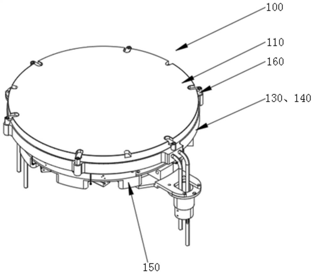
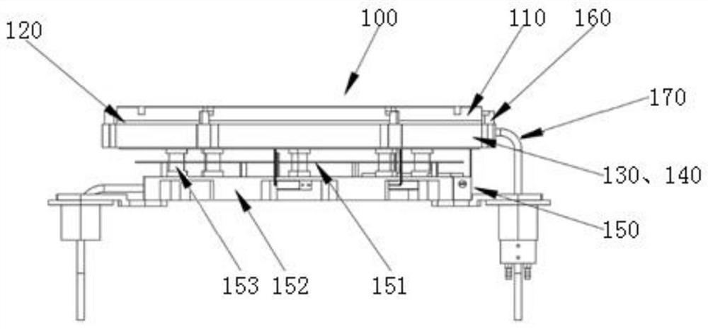
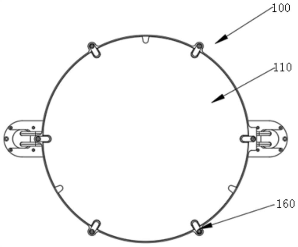
[0025] An embodiment of the present invention provides a bonding pad 100 for wafer bonding, such as Figure 1-4 As shown, the bonding pad 100 includes a pressure plate 110, a graphite layer 120, a heating plate 130, a cooling plate 140, and a heat insulating layer 150 from the inside to the outside in sequence, and the heat insulating layer 150 includes a reflective screen 151 and a substrate 152, and the substrate 152 is set On the outside of the reflective screen 151 , a cooling medium circulation channel is arranged in the substrate 152 .
[0026] When the bonding pad used for wafer bonding of the present invention is used, the upper and lower bonding pads are arranged symmetrically, and the upper and lower wafers are placed between the two bonding pa...
PUM
| Property | Measurement | Unit |
|---|---|---|
| Thickness | aaaaa | aaaaa |
| Flatness | aaaaa | aaaaa |
Abstract
Description
Claims
Application Information
 - Generate Ideas
- Intellectual Property
- Life Sciences
- Materials
- Tech Scout
- Unparalleled Data Quality
- Higher Quality Content
- 60% Fewer Hallucinations
Browse by: Latest US Patents, China's latest patents, Technical Efficacy Thesaurus, Application Domain, Technology Topic, Popular Technical Reports.
© 2025 PatSnap. All rights reserved.Legal|Privacy policy|Modern Slavery Act Transparency Statement|Sitemap|About US| Contact US: help@patsnap.com