Memory and forming method thereof

A memory and storage array technology, which is applied in the manufacture of electric solid-state devices, semiconductor devices, semiconductor/solid-state devices, etc., can solve the problems of increasing process complexity and negative effects, and achieve improved metal distribution uniformity, increased process costs, and improved storage. effect of density

Pending Publication Date: 2020-12-08
CHANGXIN MEMORY TECH INC
View PDF0 Cites 0 Cited by
  • Summary
  • Abstract
  • Description
  • Claims
  • Application Information

AI Technical Summary

Problems solved by technology

[0003] Existing methods to increase the density and capacity of DRAM are to simultaneously form logic devices and storage devices on a single wafer, which inevitably requires continuous reduction in device size on a limited wafer area, increasing process complexity and reducing device size. Negative effect of

Method used


Image

  • Memory and forming method thereof
  • Memory and forming method thereof
  • Memory and forming method thereof

Examples


Embodiment Construction

[0028] The specific implementation of the memory provided by the present invention and its forming method will be described in detail below in conjunction with the accompanying drawings.

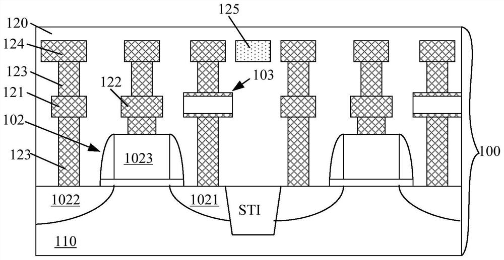
[0029] Please refer to Figure 1 to Figure 5 , is a structural schematic diagram of the formation process of the memory according to a specific embodiment of the present invention.

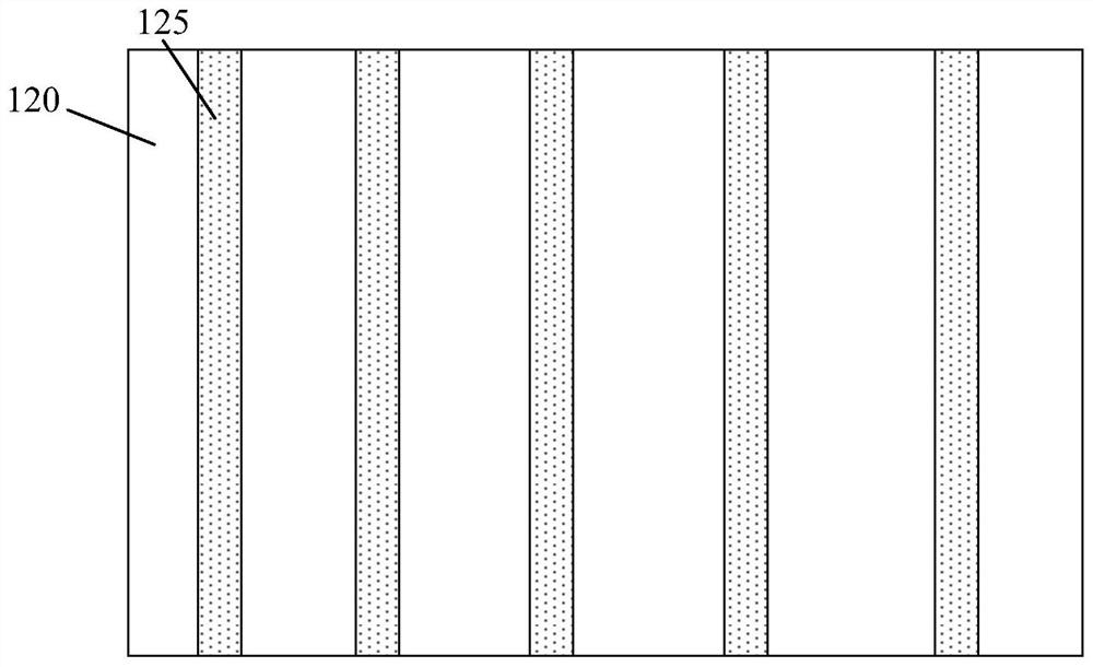
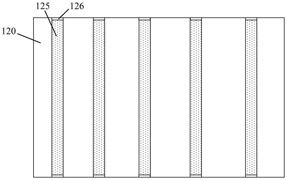
[0030] Please refer to figure 1 , providing a first substrate 100, the first substrate 100 includes a first substrate 110, a storage array formed on the front surface of the first substrate 110, and a first dielectric layer 120 covering the storage array.

[0031] The first substrate 110 is a semiconductor substrate, such as a single crystal silicon substrate, a silicon germanium substrate, a silicon-on-insulator substrate, and the like. The first substrate 110 has a shallow trench isolation structure (STI, Shallow Trench Isolation).

[0032] In this specific implementation manner, the storage array is a DRAM...


PUM


Abstract

The invention relates to a memory and a forming method thereof, and the memory comprises: a first base which comprises a first substrate, wherein a storage array formed on the front surface of the first substrate, and a first dielectric layer covering the storage array; a second base which comprises a second substrate, a logic circuit formed on the front surface of the second substrate and a second dielectric layer covering the logic circuit; and a metal heat dissipation line which is formed in the first dielectric layer and / or the second dielectric layer, wherein the first base and the secondbase are connected in a stacked and bonded mode. The storage density of the memory is improved.

Description

technical field [0001] The invention relates to the technical field of semiconductors, in particular to a memory and a forming method thereof. Background technique [0002] DRAM (Dynamic Random Access Memory, Dynamic Random Access Memory) technology is an important storage technology for integrated circuits. In order to increase the density and capacity of DRAM memory, the DRAM process is becoming more and more complex, and the size of devices is constantly shrinking. The negative effect of the device is also increasing. [0003] Existing methods to increase the density and capacity of DRAM are to simultaneously form logic devices and storage devices on a single wafer, which inevitably requires continuous reduction in device size on a limited wafer area, increasing process complexity and reducing device size. negative effect. [0004] How to further increase the density and capacity of DRAM and avoid negative effects is an urgent problem to be solved at present. Contents...

Claims


Application Information

Patent Timeline
IPC IPC(8): H01L27/108H01L23/367H01L21/8242
CPCH01L23/3677H10B12/31H10B12/48
Inventor 王连红
Owner CHANGXIN MEMORY TECH INC
Why Eureka
Try Eureka