Optical device and application thereof

An optical device and red light technology, applied in the field of far-red light optics, can solve the problem of difficult controllable adjustment of optical power, and achieve the effects of excellent reliability, reduced packaging cost, and high luminous efficiency

Active Publication Date: 2020-12-08
GRIREM ADVANCED MATERIALS CO LTD +1
View PDF6 Cites 1 Cited by
  • Summary
  • Abstract
  • Description
  • Claims
  • Application Information

AI Technical Summary

Problems solved by technology

At present, the main problem of this implementation method is: the optical power of far-red light still needs to be further improved, and the optical power in the 350-680nm band is difficult to achieve controllable adjustment

Method used


Image

  • Optical device and application thereof
  • Optical device and application thereof
  • Optical device and application thereof

Examples


Embodiment 1

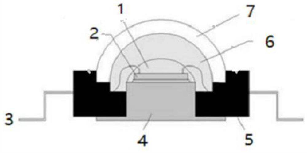
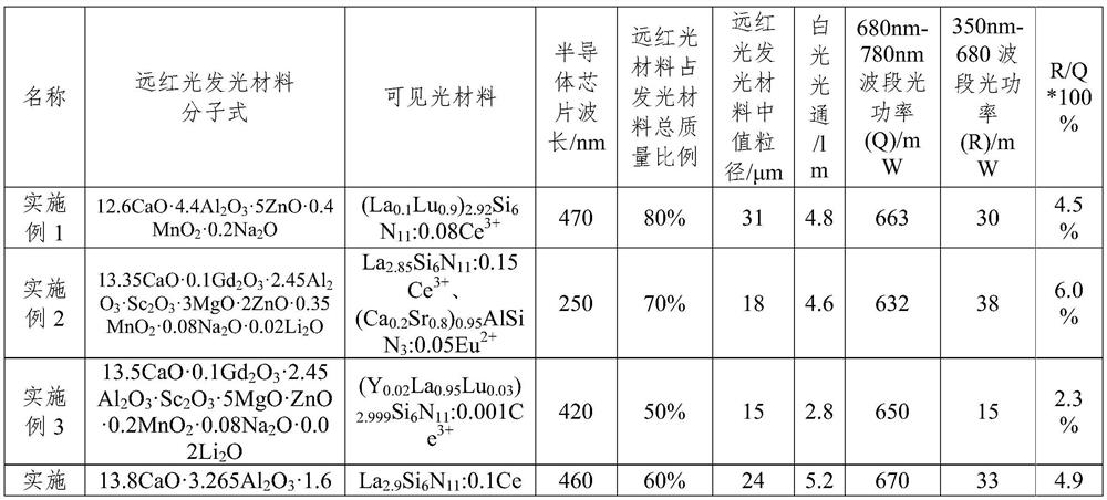
[0070] c. An optical device comprising a blue LED chip with a wavelength of 470nm and a molecular formula of 12.6CaO·4.4Al 2 o 3 5ZnO 0.4MnO 2 0.2Na 2 The far-red luminescent material of O, the molecular formula is (La 0.1 Lu 0.9 ) 2.92 Si 6 N 11 :0.08Ce 3+ The visible light luminescent material; wherein the far-red luminescent material accounts for 80% of the total mass of the total luminescent material, and the D50 particle size of the far-red luminescent material is 31 μm. In this example, the visible light luminescent material and silica gel were uniformly mixed at a mass ratio of 0.4:1, stirred, and defoamed to obtain a visible light fluorescence conversion layer mixture, and the mixture was covered on the surface of the LED chip layer by spraying, and baked It is cured into a visible light fluorescent layer. Then, the far-red light-emitting material and silica gel are mixed and evenly covered on the visible light fluorescence conversion layer according to the ma...

Embodiment 4

[0072] Embodiment 4 An optical device comprising a blue LED chip with a wavelength of 460nm and a molecular formula of 13.8CaO·3.265Al 2 o 3 1.635Ga 2 o 3 · MgO · 5ZnO · 0.2MnO 2 0.06K 2 O 0.04Li 2 The far-red luminescent material of O, the molecular formula is La 2.9 Si 6 N 11 :0.1Ce 3+ The visible light luminescent material; wherein the far-red luminescent material accounts for 60% of the total mass of the total luminescent material, and the D50 particle size of the far-red luminescent material is 24 μm. In this example, the visible light luminescent material and silica gel were uniformly mixed at a mass ratio of 0.4:1, stirred, and degassed to obtain a visible light fluorescence conversion layer mixture, and the mixture was covered on the surface of the LED chip layer by dispensing. Bake it to solidify into a visible light fluorescent layer. Then, the far-red light-emitting material and silica gel are mixed and evenly covered on the visible light fluorescence conv...

Embodiment 7

[0075] An optical device comprising a blue LED chip with a wavelength of 460nm and a molecular formula of 13.99CaO·3.995Al 2 o 3 · Ga 2 o 3 0.5MgO 5.5ZnO 0.01MnO 2 0.005K 2 The far-red luminescent material of O, the molecular formula is Sr 1.9999 Si 5 N 8 :0.0001Eu 2+ The visible light luminescent material; wherein the far-red luminescent material accounts for 80% of the total mass of the total luminescent material, and the D50 particle size of the far-red luminescent material is 26 μm. Mix the far-red luminescent material and silica gel in this embodiment evenly according to the mass ratio of 1.5:1, stir and defoam to obtain the visible light fluorescence conversion layer mixture, and cover the mixture on the surface of the LED chip layer by dispensing. Baking makes it solidify into a visible light fluorescent layer. Then, the visible light luminescent material and silica gel are mixed according to the mass ratio of 0.4:1 and evenly covered on the far-red fluorescenc...


PUM

PropertyMeasurementUnit
particle diameteraaaaaaaaaa

Abstract

The invention relates to an optical device and application thereof, the optical device comprises a light source and a luminescent material layer, the luminescent material layer contains a far-red luminescent material and a visible luminescent material, the far-red luminescent material is of a Ca14Al10Zn6O35 structure, and the molecular formula of the far-red luminescent material is aAO. zZ2O3. eE2O3. gGO.hMnO2. mM2O. According to the device, the same light source is used for achieving efficient light emitting of far-red light and visible light at the same time, the packaging process is greatlysimplified, the packaging cost is reduced, the device has the advantages of being high in light emitting efficiency, excellent in reliability and the like, meanwhile, spectrum components are adjustable and controllable, and a soft visual effect can be achieved; the device has great application prospects in the fields of security monitoring, environment light sources, full-spectrum healthy illumination, ultrahigh color gamut backlight source display and the like.

Description

technical field [0001] The invention relates to the technical field of far-red light optics, in particular to an optical device including a light source, a far-red light luminescent material and a visible light luminescent material and an application thereof. Background technique [0002] In recent years, the application of far-red light in security monitoring, ultra-high color gamut backlight display, green and healthy lighting, plant lighting, environmental light source and other fields has become the focus of the industry. Among them, far-red light LED has good directivity and low power consumption. And a series of advantages such as small size have become the focus of international research. At present, there are only corresponding far-red light semiconductor chips on the market that can meet the above-mentioned applications. For example, far-red light chips in the 710-730nm and 750nm bands are mainly used in the security field. In particular, in order to perform light ...

Claims


Application Information

Patent Timeline
Patent Type & Authority Applications(China)
IPC IPC(8): H01L33/50C09K11/64C09K11/80C09K11/79C09K11/59C09K11/62C09K11/56
CPCH01L33/502C09K11/643C09K11/7706C09K11/7774C09K11/0883C09K11/7734C09K11/7768
Inventor 刘荣辉高彤宇刘元红陈晓霞马小乐薛原
Owner GRIREM ADVANCED MATERIALS CO LTD
Why Eureka
Try Eureka