Spin polarization-coupled GaN MOSFET and preparation method thereof
A spin-polarized, bottom-up technology, applied in semiconductor/solid-state device manufacturing, semiconductor devices, electrical components, etc. Spin electron spin direction and channel current and other issues
- Summary
- Abstract
- Description
- Claims
- Application Information
AI Technical Summary
Problems solved by technology
Method used
Image


Examples
Embodiment Construction
[0035] The invention will be described in further detail below in conjunction with the accompanying drawings.
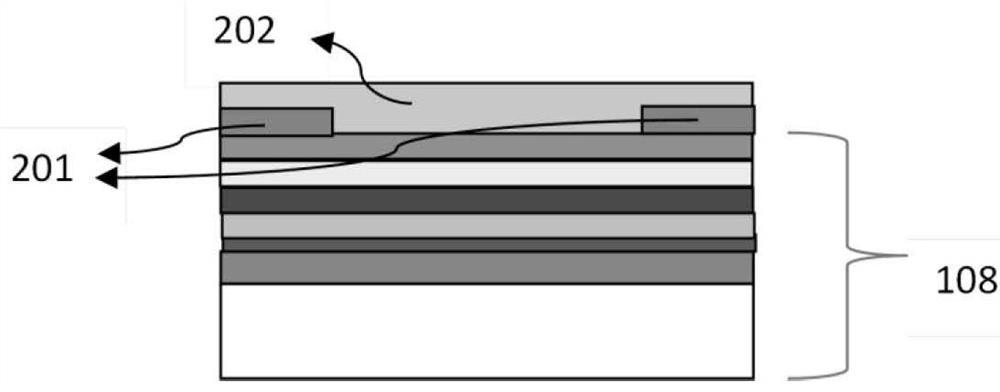
[0036] In the present invention, the magnetized film is sputtered on the surface of the barrier layer of the complete epitaxial structure of the GaN MOSFET as the underlying layer of the grid. The magnetized film is composed of metal oxide medium, ferromagnetic material and metal material. The gate and barrier layer under the magnetization film can produce field effect characteristics. The gate formed by the magnetization film has vertical magnetization or in-plane magnetization, which will generate spin polarization coupling to the electrons in the channel; at the same time, because the gate has field effect modulation characteristics for the two-dimensional electron gas in the channel, the multilayer The film gate metal has both spin polarization coupling characteristics and field effect modulation characteristics for the two-dimensional electron gas in the channe...
PUM
 Abstract
Description
Claims
Application Information