Antenna packaging structure and manufacturing method thereof

A technology of packaging structure and manufacturing method, applied in the direction of antenna support/mounting device, antenna, slot antenna, etc., can solve the problems of reducing antenna radiation performance, antenna cavity height instability, poor antenna performance, etc.

CN112074989BActive Publication Date: 2021-10-26HUAWEI TECH CO LTD
11 Cites 0 Cited by

Patent Information

Authority / Receiving Office
CN · China
Patent Type
Patents(China)
Current Assignee / Owner
Publication Date
2021-10-26

Smart Images

  • Figure 1
    Figure 1
  • Figure 2
    Figure 2
  • Figure 3
    Figure 3
Patent Text Reader

Abstract

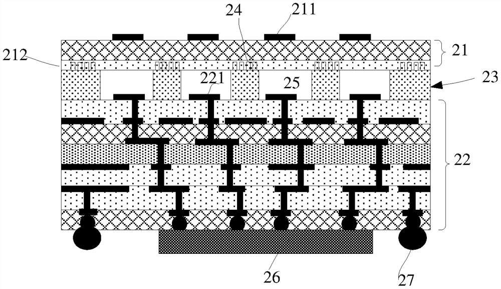
The application discloses an antenna packaging structure and a manufacturing method thereof. In the antenna packaging structure, a plurality of support blocks spaced apart from each other are arranged between the first substrate and the second substrate, and an antenna cavity is formed between every two adjacent support blocks. Thus, the height of the support block determines the height of the antenna cavity. Because the plurality of support blocks spaced apart from each other are located between the first substrate and the second substrate, and at least one of the first substrate and the second substrate is bonded to the plurality of support blocks spaced apart from each other through an adhesive layer together. Moreover, the plurality of support blocks spaced apart from each other will not experience high-temperature metal melting, and they can maintain high stability even after multiple high-temperature thermal cycles. Therefore, the antenna packaging structure has a relatively stable antenna cavity height, Thus, it has better antenna performance.
Need to check novelty before this filing date? Find Prior Art

Description

technical field

[0001] The present application relates to the technical field of antenna packaging, and in particular to an antenna packaging structure and a manufacturing method thereof. Background technique

[0002] With the advent of the 5G high-speed communication era and the development of VR (Virtual Reality, virtual reality), millimeter wave communication has gradually become the mainstream. The design and application requirements of millimeter wave antennas are also becoming more and more vigorous.

[0003] Since the length of the transmission path in the millimeter wave frequency band has a great influence on the signal amplitude loss, the traditional IC (Integrated Circuit, integrated circuit) plus PCB (Printed Circuit Board, printed circuit board) plus antenna architecture mode has gradually been unable to meet the needs of the millimeter wave frequency band. Performance requirements for short transmission paths.

[0004] In addition, the wavelength of the milli...

Examples

Embodiment Construction

[0045] In an existing AiP antenna package structure, the antenna and the chip are directly manufactured in one package.

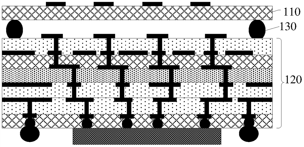
[0046] In the existing AiP antenna packaging structure, such as figure 1 As shown, the upper and lower substrates 110 and 120 are welded together by solder balls 130 , and the height of the solder balls 130 controls the distance between the upper and lower substrates 110 and 120 , that is, the height of the antenna cavity.

[0047] However, the solder balls are thermally unstable, and metal melting will occur at high temperature, resulting in highly unstable solder balls, and thus unstable distance between the upper and lower substrates.

[0048] In order to solve the problem of unstable distance between the upper and lower substrates in the AiP antenna packaging structure, the present application provides a new antenna packaging structure. In the antenna packaging structure, a plurality of support blocks spaced apart from each other are arranged between t...