Semiconductor light emitting element and light emitting device

A light-emitting element and semiconductor technology, which is applied in the direction of semiconductor devices, electrical components, circuits, etc., can solve the problems of terminal failure, electrode strip-shaped part and current blocking layer are easy to deviate, etc., to improve reliability, improve ESD performance, improve The effect of excessive concentration of charge distribution

Pending Publication Date: 2020-12-15
XIAMEN SANAN OPTOELECTRONICS CO LTD
View PDF0 Cites 3 Cited by
  • Summary
  • Abstract
  • Description
  • Claims
  • Application Information

AI Technical Summary

Problems solved by technology

However, charges tend to concentrate near the end of the electrode strip, and it is easy to deviate between the electrode strip and the current blocking layer due to the inaccurate alignment of the mask pattern. Failed nearby

Method used


Image

  • Semiconductor light emitting element and light emitting device
  • Semiconductor light emitting element and light emitting device
  • Semiconductor light emitting element and light emitting device

Examples


Embodiment 1

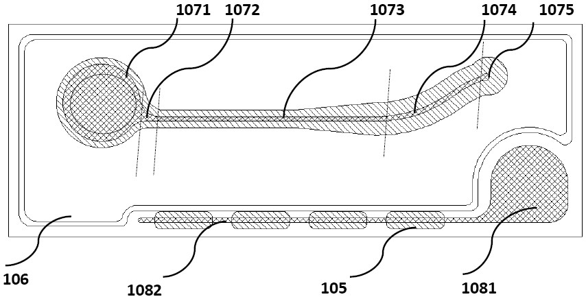
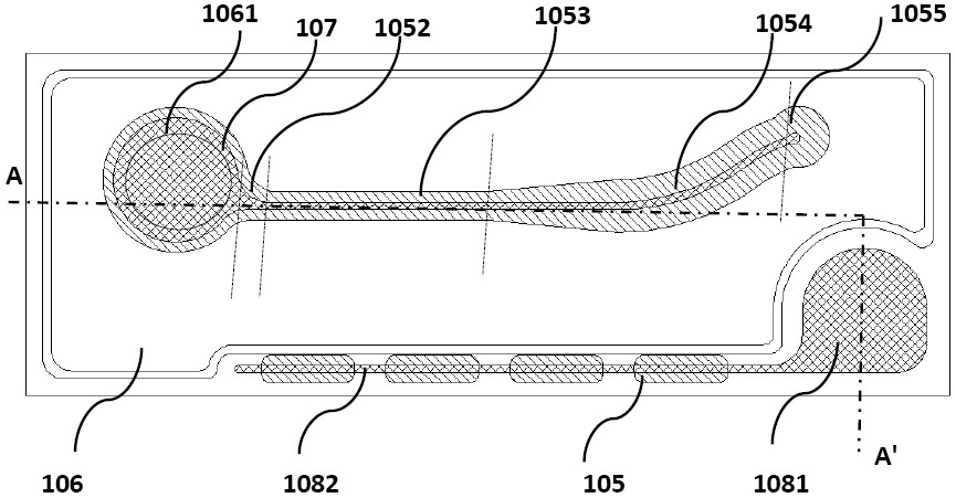
[0030] Figure 1~2 A top view of a semiconductor light emitting element according to the first embodiment of the present invention. image 3 for figure 1 A schematic diagram of the local structure of the semiconductor light-emitting element. Figure 4 for figure 1 The cross-sectional view of the semiconductor light-emitting element along the line A-A'.

[0031] In view of the above-mentioned technical problems of the existing semiconductor light-emitting elements, the present invention proposes to improve the shape of the lower current blocking layer near the end of the first metal electrode extension bar, that is, for the design of the first metal electrode extension bar including the extension section and the end, The strip-shaped portion of the current blocking layer located below part of the extension section has a widening portion that gradually widens along the extending direction gradually away from the first metal electrode pad. This can improve the excessive conc...

Embodiment 2

[0088] Such as Figure 7~8 As shown, this example provides a semiconductor light-emitting element with another electrode shape, which is different from the semiconductor light-emitting element of Embodiment 1, wherein the curved extension part replaces the outer folded line extension 1074', and the folded line extension 1074' is deviated from the straight line The extension part 1073 extends in a straight line with a fixed extension direction.

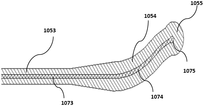
[0089] Wherein, in an exemplary embodiment, the first strip-shaped portion of the current blocking layer 105 includes a first length portion 1053, a second length portion 1054, and an enlarged end portion 1055 corresponding to a straight line extension 1073 , an arc extension 1074 and an end 1075 below.

[0090] Or as an exemplary embodiment, such as Figure 8 As shown, the first strip portion of the current blocking layer 105 includes a first length portion 1053 correspondingly located below a straight line extending section 1073, a...

Embodiment 3

[0093] This embodiment provides a semiconductor light-emitting element with another electrode shape, which is different from the semiconductor light-emitting element in Embodiment 1, and the number of first metal electrode extension strips included in the first metal electrode may be more than two. Wherein at least two first metal electrode extension strips successively include a straight line extension section, an arc extension section (or a broken line extension section) and an end in a direction gradually approaching the second metal electrode pad. One end of the straight line extension is connected to an arc extension or a broken line extension; the arc extension or the break line extension deviates from the extension direction of the straight line extension, and the arc extension is a curved line with a fixed or unfixed The arc shape of the radius of curvature, the extension of the broken line is a straight line extension, and has a fixed extension direction.

[0094] Spe...


PUM

PropertyMeasurementUnit
widthaaaaaaaaaa

Abstract

A semiconductor light emitting element includes: a first conductivity type semiconductor layer, a second conductivity type semiconductor layer, and an active layer therebetween; a current blocking layer, comprising a strip-shaped part arranged on a local surface of the first conductive type semiconductor layer; a first metal electrode, comprising a first metal electrode pad and a first metal electrode extension strip extending out of the first metal electrode pad, and the first metal electrode extension strip being located on the strip-shaped part of the current blocking layer; the first metalelectrode extension strip comprises an extension section and an end part; and the strip-shaped part of the current blocking layer, which is positioned below part of the extension section, is providedwith a widening part which is gradually widened along the extension direction which is gradually far away from the first metal electrode pad.

Description

technical field [0001] Exemplary embodiments of the present disclosure relate to a semiconductor light emitting element (LED chip), and more particularly, to a semiconductor light emitting element with high reliability. Background technique [0002] Generally, semiconductor light-emitting elements, also known as light-emitting diodes (LED chips), include a first conductivity type semiconductor layer that supplies holes, a second conductivity type semiconductor layer that supplies electrons, and a semiconductor layer interposed between the first conductivity type semiconductor layer and the second conductivity type semiconductor layer. The light-emitting layer between the layers, wherein the first conductive type semiconductor layer is a p-type layer, and the second conductive type semiconductor layer is an n-type layer. The first electrode and the second electrode are respectively formed on the semiconductor layer of the first conductivity type and the semiconductor layer of...

Claims


Application Information

Patent Timeline
Patent Type & Authority Applications(China)
IPC IPC(8): H01L33/14H01L33/36H01L33/38
CPCH01L33/14H01L33/36H01L33/38H01L33/145H01L33/382
Inventor 杨人龙张平
Owner XIAMEN SANAN OPTOELECTRONICS CO LTD
Why Eureka
Try Eureka