Defect detection system and method

A detection system and defect detection technology, which is applied in the field of defect detection, can solve problems such as wafer surface influence and chip quality pollution, and achieve the effects of improving accuracy and reliability, eliminating test uncertainty, and avoiding the reduction of signal-to-noise ratio

Pending Publication Date: 2020-12-25
HANGZHOU YUANSE TECH LTD
View PDF0 Cites 2 Cited by
  • Summary
  • Abstract
  • Description
  • Claims
  • Application Information

AI Technical Summary

Problems solved by technology

There may also be various pollutions on the surface of the wafer that affect the quality of the chip.

Method used


Image

  • Defect detection system and method
  • Defect detection system and method
  • Defect detection system and method

Examples


Embodiment Construction

[0039] The following will clearly and completely describe the technical solutions in the embodiments of the present invention with reference to the accompanying drawings in the embodiments of the present invention. Obviously, the described embodiments are only some, not all, embodiments of the present invention. Based on the embodiments of the present invention, all other embodiments obtained by persons of ordinary skill in the art without making creative efforts belong to the protection scope of the present invention.

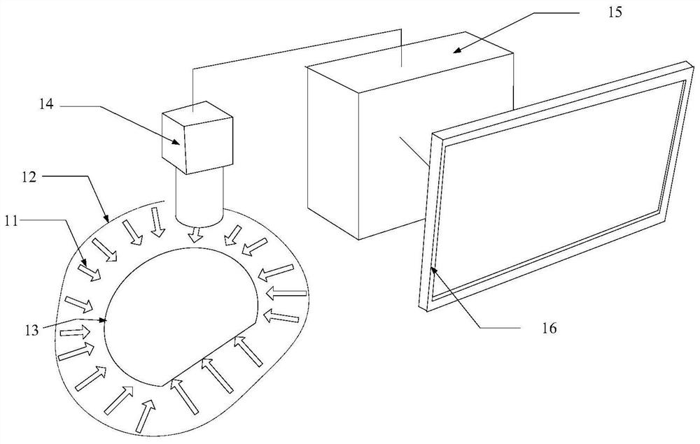
[0040] As mentioned in the background technology, the effect of wafer defect detection directly affects all aspects of semiconductor processing and preparation of control chips, so realizing low-cost and high-sensitivity wafer defect detection is an urgent problem to be solved in the field of wafer detection technology. Moreover, in order to meet customer requirements, it is also necessary to achieve high-throughput requirements. Most importantly, different typ...


PUM

PropertyMeasurementUnit
refractive indexaaaaaaaaaa

Abstract

The invention discloses a defect detection system and method. According to the technical scheme, detection light is guided into a to-be-detected structural part from the side wall of the to-be-detected structural part, defects on the surface and in the to-be-detected structural part are detected according to the total internal reflection principle, and the problem that the signal-to-noise ratio isreduced due to reflection of any surface light is avoided. Compared with a traditional optical detection method, the defect detection method has the advantages that the test uncertainty caused by angle sensitivity of a camera and a light source is eliminated, due to the fact that the direction and angle range of total internal reflection are large, the defects with random forms can be directly exposed under the condition of no background light, and the precision and reliability of defect detection are greatly improved.

Description

technical field [0001] The present invention relates to the technical field of defect detection, and more specifically, to a defect detection system and method. Background technique [0002] The control chip is one of the main components of electronic equipment to realize various functions. The wafer is the substrate for making the control chip. In order to avoid defects in the final control chip, it is very important to make a flat and particle-free wafer. Wafers are cut from silicon ingots. When the raw materials are in the ingot casting process, crystallization defects will occur during crystal growth and subsequent process steps, so the final formed wafers may have the following defects, such as simple particles, crystal-derived particles or pits (COP), residue and scratches. There may also be various pollutions on the surface of the wafer that affect the quality of the chip. [0003] Therefore, the challenge of advanced wafer technology is to reduce and control the i...

Claims


Application Information

Patent Timeline
Patent Type & Authority Applications(China)
IPC IPC(8): G01N21/95
CPCG01N21/9505
Inventor 季中陈荣湾杨振辉
Owner HANGZHOU YUANSE TECH LTD
Why Eureka
Try Eureka