Novel multi-dimensional multifunctional superconducting superlattice large-scale integrated circuit

A large-scale integrated circuit and superlattice technology, applied in circuits, electrical components, electrical solid devices, etc., can solve the problems of low integration, poor stability of integrated circuits, poor testability, etc., to avoid mutual interference and integration. The effect of improving and enhancing reliability

Active Publication Date: 2020-12-25
林和
View PDF4 Cites 0 Cited by
  • Summary
  • Abstract
  • Description
  • Claims
  • Application Information

AI Technical Summary

Problems solved by technology

[0003] The present invention provides a novel multi-dimensional multifunctional superconducting superlattice large-scale integrated circuit, which is used to solve the problems of poor stability, poor testability, low integration and high cost in the integrated circuits of existing devices:

Method used


Image

  • Novel multi-dimensional multifunctional superconducting superlattice large-scale integrated circuit
  • Novel multi-dimensional multifunctional superconducting superlattice large-scale integrated circuit
  • Novel multi-dimensional multifunctional superconducting superlattice large-scale integrated circuit

Examples


Embodiment Construction

[0065] The preferred embodiments of the present invention will be described below in conjunction with the accompanying drawings. It should be understood that the preferred embodiments described here are only used to illustrate and explain the present invention, and are not intended to limit the present invention.

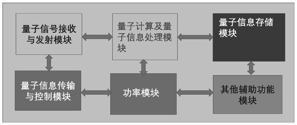
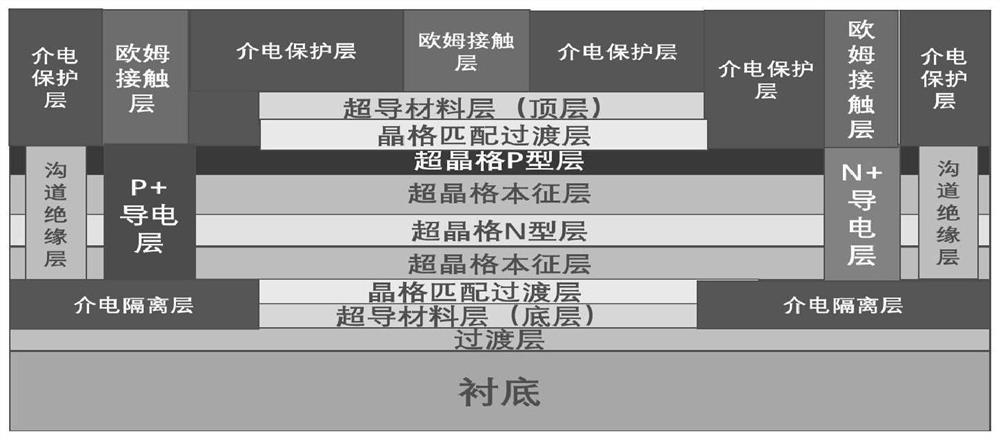
[0066] Embodiments of the present invention propose a novel multi-dimensional multifunctional superconducting superlattice large-scale integrated circuit, such as figure 1 As shown, the large-scale integrated circuit includes a substrate, a transition layer and a superconducting superlattice large-scale integrated circuit layer; the transition layer is arranged between the substrate and the superconducting superlattice large-scale integrated circuit layer between.

[0067] Wherein, the substrate is made of a silicon wafer or a compound semiconductor wafer. The compound semiconductor wafer includes materials such as gallium nitride (GaN), gallium arsonide (GaAs) or ...


PUM

PropertyMeasurementUnit
sizeaaaaaaaaaa

Abstract

The invention provides a novel multi-dimensional multifunctional superconducting superlattice large-scale integrated circuit, and belongs to the technical field of integrated circuits. The large-scaleintegrated circuit comprises a substrate, a transition layer and a superconducting superlattice large-scale integrated circuit layer. The transition layer is arranged between the substrate and the superconducting superlattice large-scale integrated circuit layer. The substrate is made of a silicon wafer or a compound semiconductor wafer.

Description

technical field [0001] The invention proposes a novel multi-dimensional multifunctional superconducting superlattice large-scale integrated circuit, which belongs to the technical field of integrated circuits. Background technique [0002] The rapid development of big data, artificial intelligence and all-round digital intelligent market urgently needs new large-scale integrated circuits with high performance, high reliability and acceptable cost, especially in the fields of high-speed information processing, quantum computing and quantum communication. Quantum devices face many challenges, such as device performance stability, testability, integration and high cost. More importantly, silicon-based silicon-based large-scale integrated circuit components have become increasingly difficult to meet the special performance requirements of artificial intelligence and space age for ultra-high speed, high reliability and radiation resistance. Contents of the invention [0003] T...

Claims


Application Information

Patent Timeline
Patent Type & Authority Applications(China)
IPC IPC(8): H01L27/18
CPCH10N69/00
Inventor 林和
Owner 林和
Why Eureka
Try Eureka