

Alloy ultraviolet transparent conductive film and preparation method and application thereof
A technology of transparent conductive film and conductive film, which is applied in metal material coating process, ion implantation plating, coating, etc., can solve the problem that ultraviolet light cannot pass through, achieve good practical application prospects, low production cost, and low cost of raw materials Inexpensive and easy to get effects
- Summary
- Abstract
- Description
- Claims
- Application Information
AI Technical Summary
Problems solved by technology
Method used
Image

Examples
Embodiment 1
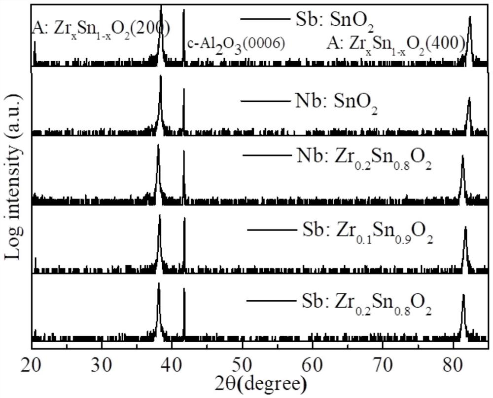
[0039] The invention provides an alloy ultraviolet transparent conductive film, which is Zr doped with A x sn 1-x o 2 n-type conductive thin film, wherein, A is Sb or Nb.
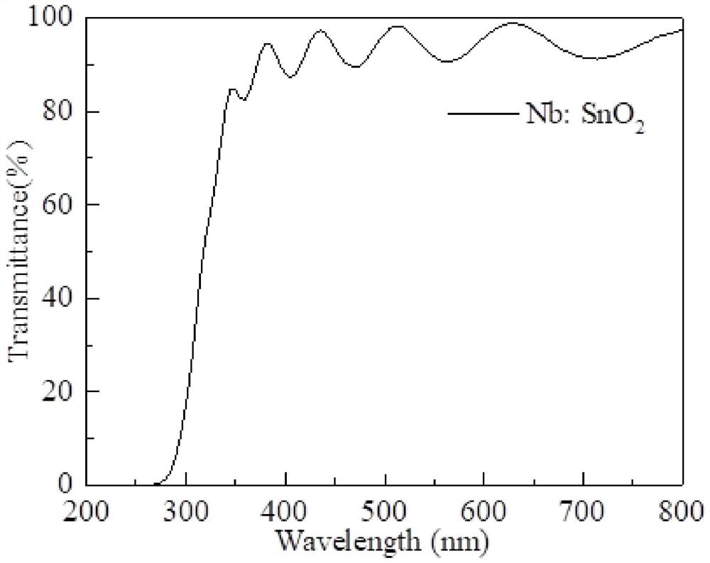
[0040] Specifically, in the embodiment of the present application, A is Nb, and x is 0, that is, the thin film in the embodiment of the present application is SnO doped with Nb 2 (Nb:SnO 2 ) n-type conductive film. Specifically, the thickness of the conductive film is 500nm.
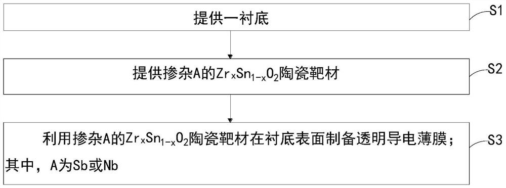
[0041] Based on the same inventive concept, the present invention also provides the preparation method of the above-mentioned alloy ultraviolet transparent conductive film, such as figure 1 shown, including the following steps:
[0042] S1, providing a substrate;
[0043] S2, providing Zr doped with A x sn 1-x o 2 ceramic target;
[0044] S3, using Zr doped with A x sn 1-x o 2 Prepare a transparent conductive film on the surface of the substrate with a ceramic target;
[0045] Wherein, A is Sb or Nb.
[0046]It should ...
Embodiment 2
[0055] The invention provides an alloy ultraviolet transparent conductive film, which is Zr doped with A x sn 1-x o 2 n-type conductive thin film, wherein, A is Sb or Nb.
[0056] Specifically, in the embodiment of the present application, A is Nb, and x is 0.2, that is, the film in the embodiment of the present application is Zr doped with Nb 0.2 sn 0.8 o 2 (Nb:Zr 0.2 sn 0.8 o 2 ) n-type conductive film. Specifically, the thickness of the conductive film is 500nm.
[0057] It should be noted that SnO 2 The band gap is 3.6eV, ultraviolet light cannot pass through, and ZrO 2 The band gap is greater than 5.5eV, by adding SnO 2 with ZrO 2 Alloying to adjust the band gap so that it can meet the transmission of ultraviolet light. Undoped SnO 2 The conductivity of the film mainly depends on oxygen vacancies, and the concentration of oxygen vacancies is often difficult to control. Moreover, the larger the band gap of the semiconductor, the more difficult its intrinsic e...
Embodiment 3
[0072] The invention provides an alloy ultraviolet transparent conductive film, which is Zr doped with A x sn 1-x o 2 n-type conductive thin film, wherein, A is Sb or Nb.
[0073] Specifically, in the embodiment of the present application, A is Sb, and x is 0.1, that is, the film in the embodiment of the present application is Zr doped with Sb 0.1 sn 0.9 o 2 (Sb:Zr 0.1 sn 0.9 o 2 ) n-type conductive film. Specifically, the thickness of the conductive film is 400nm.
[0074] Based on the same inventive concept, the present invention also provides a method for preparing the above-mentioned alloy ultraviolet transparent conductive film, comprising the following steps:
[0075] S1, providing a substrate;
[0076] S2, providing Zr doped with A x sn 1-x o 2 ceramic target;
[0077] S3, using Zr doped with A x sn 1-x o 2 Prepare a transparent conductive film on the surface of the substrate with a ceramic target;
[0078] Wherein, A is Sb or Nb.
[0079] It should b...
PUM
| Property | Measurement | Unit |
|---|---|---|
| thickness | aaaaa | aaaaa |
| diameter | aaaaa | aaaaa |
| band gap | aaaaa | aaaaa |
Abstract
Description
Claims
Application Information