Array substrate, display panel and electronic equipment

An array substrate and electrode technology, applied in the display field, can solve problems such as reducing the stability of optical sensors, deep via holes, and increasing the risk of exposure and etching processes

Active Publication Date: 2021-01-08
WUHAN CHINA STAR OPTOELECTRONICS TECH CO LTD
View PDF6 Cites 3 Cited by
  • Summary
  • Abstract
  • Description
  • Claims
  • Application Information

AI Technical Summary

Problems solved by technology

[0003] At present, the optical fingerprint technology applied to organic light-emitting diodes is relatively extensive, but there are few optical fingerprint technologies applied to liquid crystal display panels. Due to the limitations of factors such as backlight and aperture ratio, it is necessary to fabricate optical sensors on array substrates, but this will cause The via hole depth between the upper conductive layer and the lower metal part is deeper, which increases the process risk in the exposure and etching process and reduces the stability of the optical sensor

Method used


Image

  • Array substrate, display panel and electronic equipment
  • Array substrate, display panel and electronic equipment
  • Array substrate, display panel and electronic equipment

Examples


Embodiment Construction

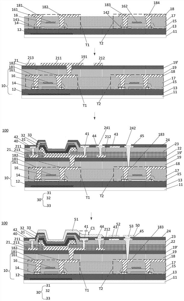
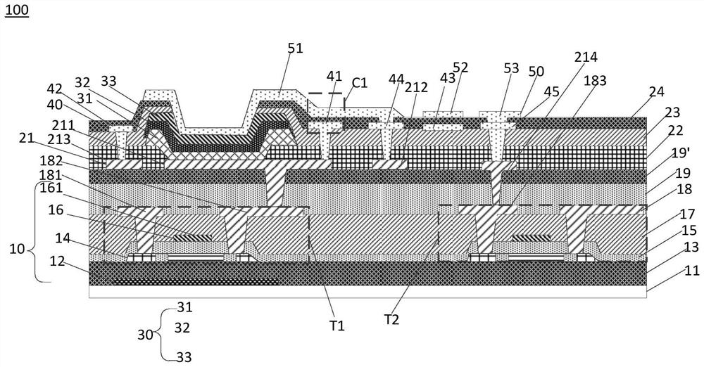
[0021] The following descriptions of the various embodiments refer to the accompanying drawings to illustrate specific embodiments in which the present invention can be practiced. The directional terms mentioned in the present invention, such as "up", "down", "front", "back", "left", "right", "inside", "outside", "side", etc., are for reference only The orientation of the attached schema. Therefore, the directional terms used are used to illustrate and understand the present invention, but not to limit the present invention. In the figures, structurally similar units are denoted by the same reference numerals.

[0022] The terms "first", "second" and the like in the description and claims of the present invention and the above drawings are used to distinguish different objects, rather than to describe a specific order. Furthermore, the terms "include" and "have", as well as any variations thereof, are intended to cover a non-exclusive inclusion.

[0023] see Figure 1 to F...


PUM


Abstract

The invention discloses an array substrate, a display panel and electronic equipment. The array substrate comprises a substrate which comprises a first conductive layer disposed on a third insulatinglayer; the first conductive layer comprises a first connecting part; the first connecting part is connected with a first metal part; a fourth insulator is arranged on the first conductive layer; a second via hole is formed in the fourth insulator; the second conducting layer is arranged on the fourth insulator and in the second via hole; the second conducting layer comprises a second electrode; the second electrode covers a PIN diode; and the second electrode is connected with the first connecting part through the second via hole. According to the array substrate, the display panel and the electronic equipment, the stability of an optical sensor can be improved.

Description

technical field [0001] The present invention relates to the field of display technology, in particular to an array substrate, a display panel and electronic equipment. Background technique [0002] The combination of optical fingerprint technology and display panel is one of the main directions at present. Its principle is to use the different intensity of light reflected by the valleys and ridges of the fingerprint to the sensing area of ​​the display panel to convert different optical signals into The electrical signal is extracted through the chip to form a key fingerprint pattern to achieve the purpose of fingerprint identification. [0003] At present, the optical fingerprint technology applied to organic light-emitting diodes is relatively extensive, but there are few optical fingerprint technologies applied to liquid crystal display panels. Due to the limitations of factors such as backlight and aperture ratio, it is necessary to fabricate optical sensors on array sub...

Claims


Application Information

Patent Timeline
Patent Type & Authority Applications(China)
IPC IPC(8): G02F1/1362G02F1/1343G02F1/1333G06K9/00
CPCG02F1/1362G02F1/136227G02F1/134363G02F1/13338G02F1/1333G06V40/1318H01L27/14603H01L27/14643H01L27/14692H01L27/14612G02F1/13685G02F1/13318G02F1/13439G06F3/0412
Inventor 艾飞宋继越宋德伟
Owner WUHAN CHINA STAR OPTOELECTRONICS TECH CO LTD
Why Eureka
Try Eureka