Intracavity wafer centering system and working method thereof
A wafer-centering technology, applied in electrical components, semiconductor/solid-state device manufacturing, circuits, etc., can solve the problem of poor etching repeatability in the edge area of the wafer
- Summary
- Abstract
- Description
- Claims
- Application Information
AI Technical Summary
Problems solved by technology
Method used
Image

Examples
Embodiment Construction
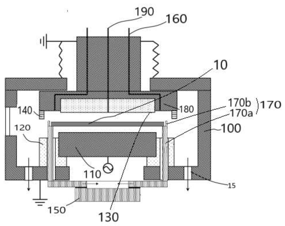
[0030] An embodiment of the present invention provides an intracavity wafer centering system, please refer to figure 1 ,include:
[0031] body cavity 100;
[0032] A wafer support platform 110 located in the main cavity 100, the surface of the wafer support platform 110 is suitable for placing a wafer 10;
[0033] A plurality of displacement holes located at the side of the wafer support platform 110 and passing through the bottom wall of the main chamber 100;
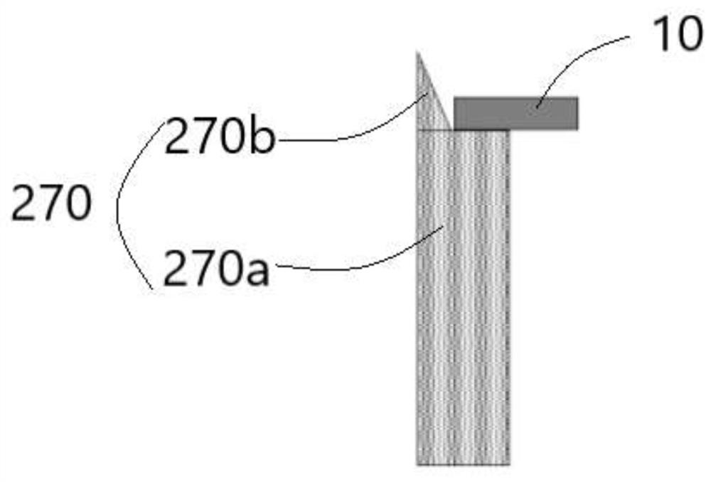
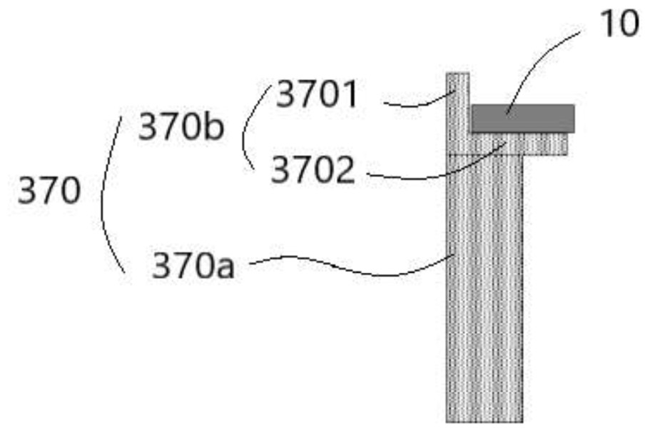
[0034] The thimbles 170 respectively located in the displacement holes, the thimbles 170 include a thimble body 170a and a limiting part 170b;
[0035] The thimble position adjusting member 150 located at the bottom of the main cavity 100 is suitable for controlling the distance between the thimble 170 and the central axis of the wafer support platform 110 , and the thimble position adjusting member 150 It is also suitable for controlling the longitudinal reciprocating movement of the thimble 170 in the displacement...
PUM
 Abstract
Description
Claims
Application Information
 - R&D Engineer
- R&D Manager
- IP Professional
- Industry Leading Data Capabilities
- Powerful AI technology
- Patent DNA Extraction
Browse by: Latest US Patents, China's latest patents, Technical Efficacy Thesaurus, Application Domain, Technology Topic.
© 2024 PatSnap. All rights reserved.Legal|Privacy policy|Modern Slavery Act Transparency Statement|Sitemap