Novel SiC GTO device with double base regions and double emitter regions
A double-emitter, double-base technology, applied in the direction of semiconductor devices, electrical components, thyristors, etc., can solve the problems of reducing gate current stability, reducing device current gain, and low emitter injection efficiency, so as to achieve small driving current, Reduced on-resistance and large current gain
- Summary
- Abstract
- Description
- Claims
- Application Information
AI Technical Summary
Problems solved by technology
Method used
Image
Examples
Embodiment 1
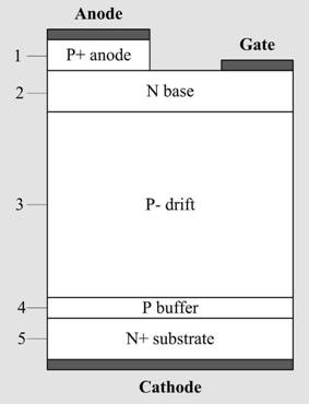
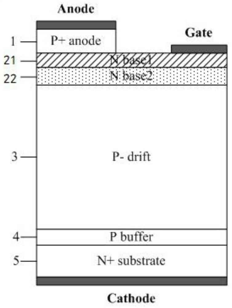
[0024] like figure 2 As shown, a new type of SiC GTO device with double base and double emitters, vertically from the anode to the cathode includes: P+ emitter 1, N-type base 2, P-type drift region 3, P-type buffer 4 and N+ type substrate 5; and the P+ emitter region 1 is connected to the device anode, the N-type base region 2 is connected to the device gate, and the N+ type substrate 5 is connected to the device cathode; the P+ emitter region 1 has a one-layer structure in the vertical direction; the N-type The base region 2 has a two-layer structure vertically, including a low-concentration doped base region 21 in contact with the P+ emitter region 1 and a high-concentration doped base region 22 in contact with the P-type drift region 3 .
[0025] In this embodiment, the concentration of the highly doped base region 22 is 1e16cm -3 .
[0026] In this embodiment, the low concentration doped base region 21 has a concentration of 3e15cm -3 .
[0027] For the SiC GTO device...
Embodiment 2
[0029] like figure 2 As shown, a new type of SiC GTO device with double base and double emitters, vertically from the anode to the cathode includes: P+ emitter 1, N-type base 2, P-type drift region 3, P-type buffer 4 and N+ type substrate 5; and the P+ emitter region 1 is connected to the device anode, the N-type base region 2 is connected to the device gate, and the N+ type substrate 5 is connected to the device cathode; the P+ emitter region 1 has a one-layer structure in the vertical direction; the N-type The base region 2 has a two-layer structure vertically, including a low-concentration doped base region 21 in contact with the P+ emitter region 1 and a high-concentration doped base region 22 in contact with the P-type drift region 3 .
[0030] In this embodiment, the concentration of the highly doped base region 22 is 5e17cm -3 .
[0031] In this embodiment, the low concentration doped base region 21 has a concentration of 1e15cm -3 .
Embodiment 3
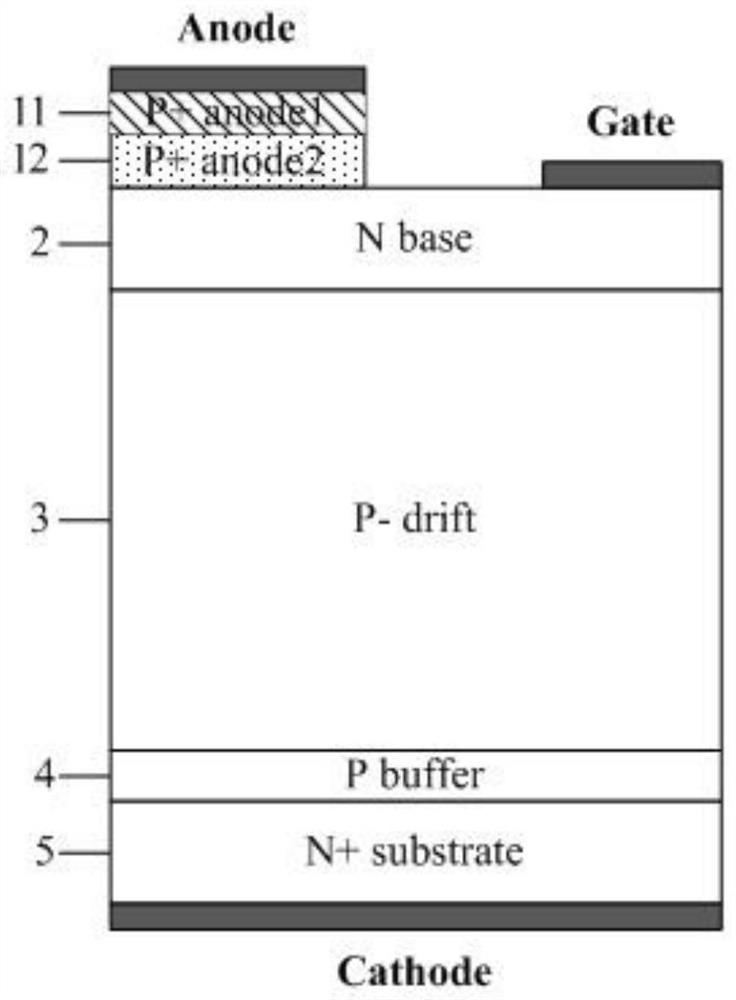
[0033] like image 3 As shown, a new type of SiC GTO device with double base and double emitters, vertically from the anode to the cathode includes: P+ emitter 1, N-type base 2, P-type drift region 3, P-type buffer 4 and N+ type substrate 5; and the P+ emitter region 1 is connected to the device anode, the N-type base region 2 is connected to the device gate, and the N+ type substrate 5 is connected to the device cathode; the N-type base region 2 has a one-layer structure in the vertical direction; P+ The emitter region 1 has a two-layer structure in the longitudinal direction, including a P+ emitter region 12 in contact with the N-type base region 3 and a P++ emitter region 11 in contact with the anode.
[0034] In this embodiment, the doping concentration of the P+ emitter region 12 is 1e19cm -3 .
[0035] In this embodiment, the doping concentration of the P++ emitter region 11 is 1e20cm -3 .
[0036] The SiC GTO anode region is used as the emitter region of the PNP typ...
PUM
 Abstract
Description
Claims
Application Information


