

Machine table for wafer cleaning machine
A cleaning machine and wafer technology, applied in electrical components, semiconductor/solid-state device manufacturing, circuits, etc., can solve problems such as wafer displacement, inability to clamp wafers, and inability to adjust the position of rectifier baffles to meet filling needs , The effect of reasonable structure design and reasonable distribution of ventilation holes
- Summary
- Abstract
- Description
- Claims
- Application Information
AI Technical Summary
Problems solved by technology
Method used
Image

Examples
Embodiment Construction
[0022] The following will clearly and completely describe the technical solutions in the embodiments of the present invention with reference to the accompanying drawings in the embodiments of the present invention. Obviously, the described embodiments are only some, not all, embodiments of the present invention. Based on the embodiments of the present invention, all other embodiments obtained by persons of ordinary skill in the art without creative efforts fall within the protection scope of the present invention.
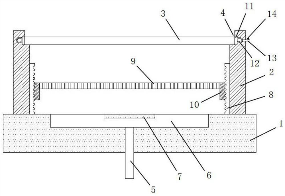
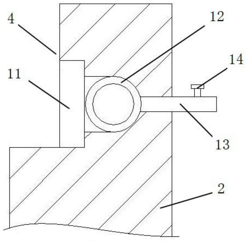
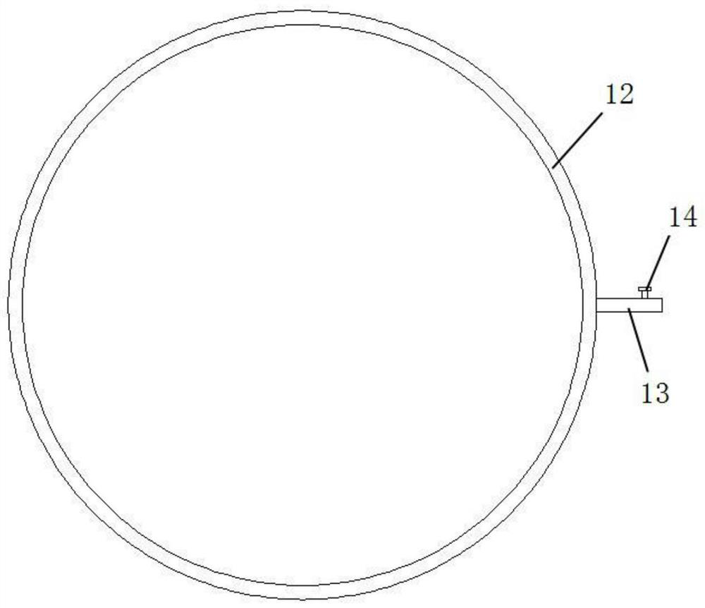
[0023] see Figure 1-3 As shown, the present embodiment is a machine table for a wafer cleaning machine, which includes a rotating base 1 , and a protective gas pipeline 5 for filling the protective gas is plugged into the center of the rotating base 1 . A receiving sleeve 2 is fixed on the upper end of the rotating base 1 , and an outer groove 4 for placing a wafer 3 is provided on the inner side of the upper end of the receiving sleeve 2 . The side end of the ou...
PUM
 Abstract
Description
Claims
Application Information