MEMS sensor and preparation method thereof
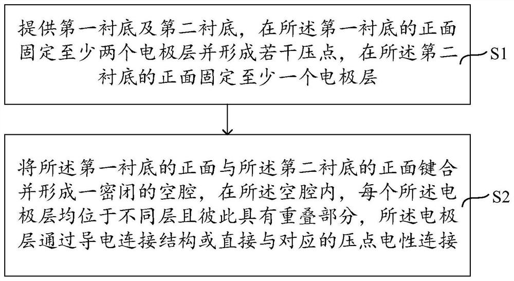
A sensor and electrode layer technology, applied in the field of MEMS sensor and its preparation, can solve the problems of complex preparation process and packaging process, low reliability of force sensor, etc.
- Summary
- Abstract
- Description
- Claims
- Application Information
AI Technical Summary
Problems solved by technology
Method used
Image
Examples
Embodiment 1
[0086] Figure 4 A schematic structural diagram of the MEMS sensor is provided for this embodiment. In this embodiment, the MEMS sensor is a force sensor, such as Figure 4 As shown, the force sensor includes a first substrate 100, a second substrate 110 and a supporting wall between the first substrate 100 and the second substrate 110, the first substrate 100 The front side is opposite to the front side of the second substrate 110, and the supporting wall together with the first substrate 100 and the second substrate 110 forms a closed cavity, wherein the first substrate 100 and the second substrate 110 respectively serve as the upper and lower surfaces of the cavity, and the supporting walls serve as the sides of the cavity.
[0087]Specifically, the support wall includes a first support layer 601, a second support layer 611 and a first conductive bonding layer 621, the first support layer 601 is formed on the front side of the first substrate 100, the The second supporti...
Embodiment 2
[0144] Figure 6 Schematic diagram of the structure of the MEMS sensor provided for this embodiment. Such as Figure 6 As shown, the difference from Embodiment 1 is that in this embodiment, two electrode layers are fixed on the front surface of the second substrate, that is, the third electrode layer 212a also has a fourth electrode layer 213a.
[0145] combine Figure 4 and Figure 6 , the fourth electrode layer 213a is located above the third electrode layer 212a, and the fourth electrode layer 213a is also fixed on the front surface of the second substrate 110 through a part of the second conductive connection structure, so There is a certain distance between the fourth electrode layer 213a and the third electrode layer 212a perpendicular to the thickness direction, so that there is an air interlayer between the fourth electrode layer 213a and the third electrode layer 212a.
[0146] The third electrode layer 212a and the fourth electrode layer 213a have an overlapping ...
Embodiment 3
[0171] Figure 7 A top view of the first substrate 100 provided in this embodiment. Such as Figure 7 and Figure 4 As shown, the difference from Embodiment 1 is that in this embodiment, the second electrode layer 202a is fixed on the front surface of the first substrate 100 through four first conductive connection structures, and the third electrode layer 212a The four second conductive connection structures are fixed on the front surface of the second substrate 110, the four first conductive connection structures are distributed at the four corners of the second electrode layer 202a, and the four second conductive connection structures are distributed at the four corners of the second electrode layer 202a. four sides of the third electrode layer 212a. The four corners of the second electrode layer 202a are respectively electrically connected to the corresponding pressure points through one of the first conductive connection structures, and the four sides of the third elec...
PUM
 Abstract
Description
Claims
Application Information


