Service life testing method for wafers
A technology of life testing and wafers, applied in the field of life testing of wafers, can solve the problems of cumbersome chemical passivation operation process, increase the production cost of enterprises, do not meet environmental protection requirements, etc., achieve high test efficiency and improve utilization rate , the effect of short measurement time
- Summary
- Abstract
- Description
- Claims
- Application Information
AI Technical Summary
Problems solved by technology
Method used
Image

Examples
Embodiment 1
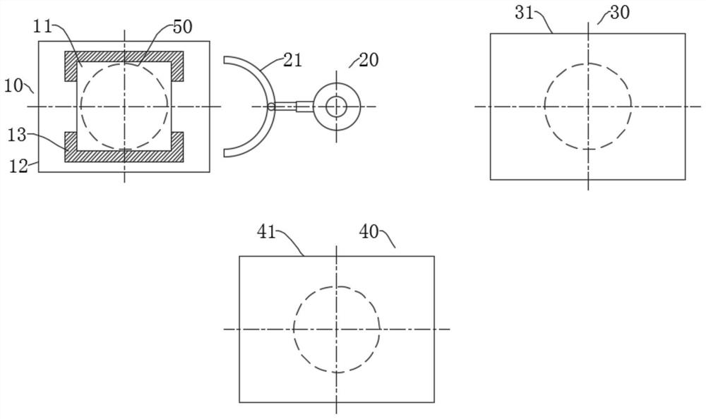
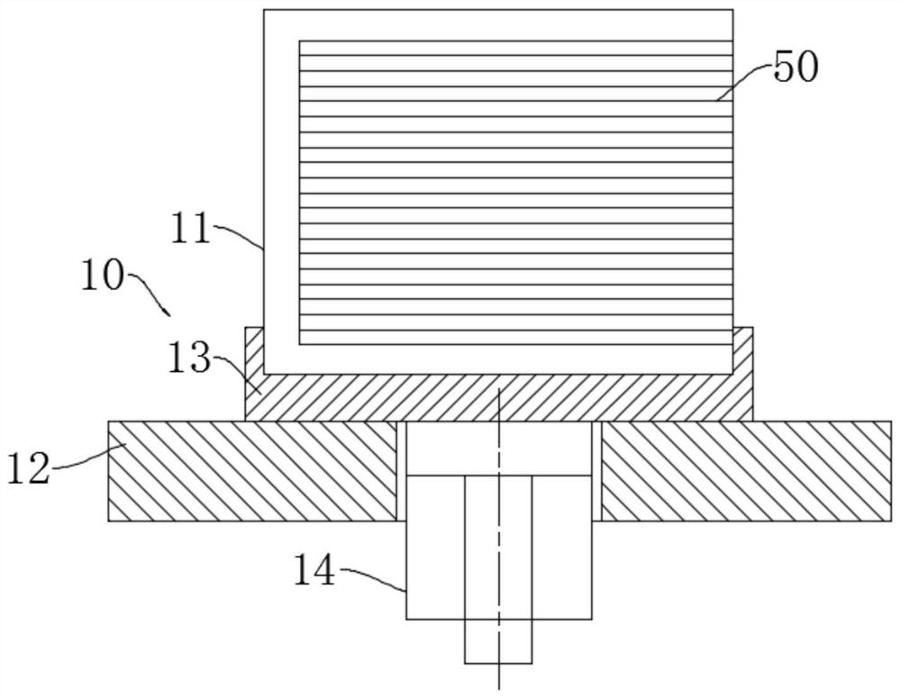
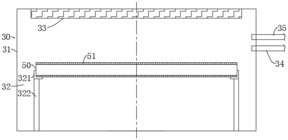
[0071] Divide the single crystal silicon rod with a diameter of 300mm into three sections from the beginning to the end, which are head 1#, middle part 2# and tail part 3#, and start from the beginning at the head 1#, middle part 2# and tail part 3# Take a number of wafers 50 from the position to the end, and mark the positions of the wafers 50 in the section, such as: 1-002 is the second piece in the head 1#, and 2-102 is the middle 2# 102nd tablet. In this embodiment, select the 2nd piece and the 102nd piece of the head 1#, namely respectively 1-002, 1-102; the 2nd piece, the 102nd piece and the 202nd piece of the middle part 2#, namely respectively 2-002, 2-102 and 2-202; the 2nd, 102nd and 202nd pieces of the tail 3#, that is, 3-002, 3-102 and 3-202 respectively. Adopt the lifetime data that above-mentioned steps obtains as shown in table 1; According to the data in table 1 simultaneously, take the position of wafer 50 in the monocrystalline silicon rod and take from head...
PUM
| Property | Measurement | Unit |
|---|---|---|
| Thickness | aaaaa | aaaaa |
Abstract
Description
Claims
Application Information
 - Generate Ideas
- Intellectual Property
- Life Sciences
- Materials
- Tech Scout
- Unparalleled Data Quality
- Higher Quality Content
- 60% Fewer Hallucinations
Browse by: Latest US Patents, China's latest patents, Technical Efficacy Thesaurus, Application Domain, Technology Topic, Popular Technical Reports.
© 2025 PatSnap. All rights reserved.Legal|Privacy policy|Modern Slavery Act Transparency Statement|Sitemap|About US| Contact US: help@patsnap.com