

Novel conductive film, preparation method thereof and touch screen
A conductive film, touch screen technology, applied in chemical instruments and methods, electronic equipment, flat products, etc., can solve the problems of poor back-end line adhesion, limited size of the middle visible area, etc., to achieve strong adhesion , excellent performance, not easy to release the effect of the film
- Summary
- Abstract
- Description
- Claims
- Application Information
AI Technical Summary
Problems solved by technology
Method used
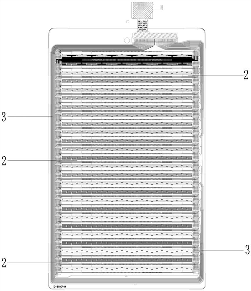
Image

Examples
Embodiment 1
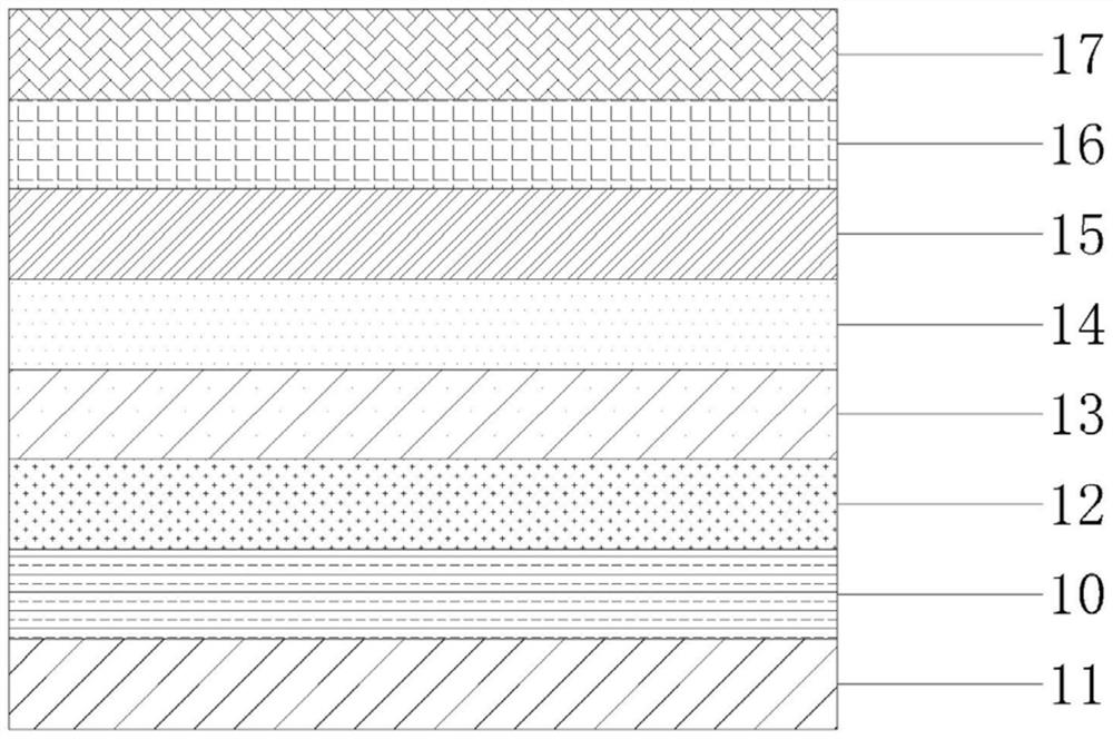
[0032] The substrate layer 10 is a PET layer, COP layer, PI layer or PC layer with a thickness of 6-200um; the underlying layer 12 is a silicon oxide layer with a thickness of 12nm; the touch layer 13 in the visible area is an indium tin oxide layer with a thickness of 22nm; the connection layer 14 is a simple silicon layer with a thickness of 5nm; the frame wiring metal layer 15 is a copper layer with a thickness of 150nm; the anti-oxidation layer 16 is a copper-nickel-titanium alloy layer with a thickness of 6nm; the other side of the substrate layer 10 A PET protective film 11 is pasted on it, and a CPP protective film 17 is pasted on the frame wiring metal layer 15. The performance results at this time: the impedance is 0.12Ω, and the adhesion is 5B.
Embodiment 2
[0034] The substrate layer 10 is a PET layer, a COP layer, a PI layer or a PC layer with a thickness of 6-200um; the underlying layer 12 is a silicon oxide layer with a thickness of 15nm; the touch layer 13 in the visible area is an indium tin oxide layer with a thickness of 21nm; the connection layer 14 is a single silicon layer and an aluminum oxide layer, with a thickness of 15nm; the frame wiring metal layer 15 is a copper layer, with a thickness of 185nm; the anti-oxidation layer 16 is a copper-nickel-titanium alloy layer, with a thickness of 15nm; the substrate layer A PET protective film 11 is pasted on the other side of 10 , and a CPP protective film 17 is pasted on the metal layer of the frame wiring. The performance results at this time: the impedance is 0.1Ω, and the adhesion is 5B.
Embodiment 3
[0036]The substrate layer 10 is a PET layer, a COP layer, a PI layer or a PC layer with a thickness of 6-200um; the underlying layer 12 is a silicon oxide layer with a thickness of 15nm; the touch layer 13 in the visible area is an indium tin oxide layer with a thickness of 21nm; the connection layer 14 is an aluminum oxide layer with a thickness of 1nm; the frame wiring metal layer 15 is a copper layer with a thickness of 185nm; the anti-oxidation layer 16 is a copper-nickel-titanium alloy layer with a thickness of 45nm; the other side of the substrate layer 10 A PET protective film 11 is pasted on it, and a CPP protective film 17 is pasted on the metal layer of the frame wiring. The performance results at this time: the impedance is 0.1Ω, and the adhesion is 5B.
[0037] From the comparison of the experimental data, it can be concluded that when alumina is used as the connecting layer, it has better adhesion.
[0038] The following table takes Example 3 as an example, and co...
PUM
| Property | Measurement | Unit |
|---|---|---|
| thickness | aaaaa | aaaaa |
| thickness | aaaaa | aaaaa |
| thickness | aaaaa | aaaaa |
Abstract
Description
Claims
Application Information