Cascaded Circuits and Cascaded Devices Based on Gate Protection

A technology of cascading circuits and devices, applied in the direction of electric solid devices, circuits, electrical components, etc., can solve the problems of insufficient driving ability and unapplied power devices, and achieve the effect of practical value, reduced impact, and complete compatibility.

Active Publication Date: 2022-04-01
苏州英嘉通半导体有限公司
View PDF5 Cites 0 Cited by
  • Summary
  • Abstract
  • Description
  • Claims
  • Application Information

AI Technical Summary

Problems solved by technology

However, due to its special protection mechanism, the drive current of the power device must be less than the maximum gate forward current it can withstand, resulting in insufficient drive capability, making the power device unable to be used in practical switching applications

Method used


Image

  • Cascaded Circuits and Cascaded Devices Based on Gate Protection
  • Cascaded Circuits and Cascaded Devices Based on Gate Protection
  • Cascaded Circuits and Cascaded Devices Based on Gate Protection

Examples


Embodiment 1

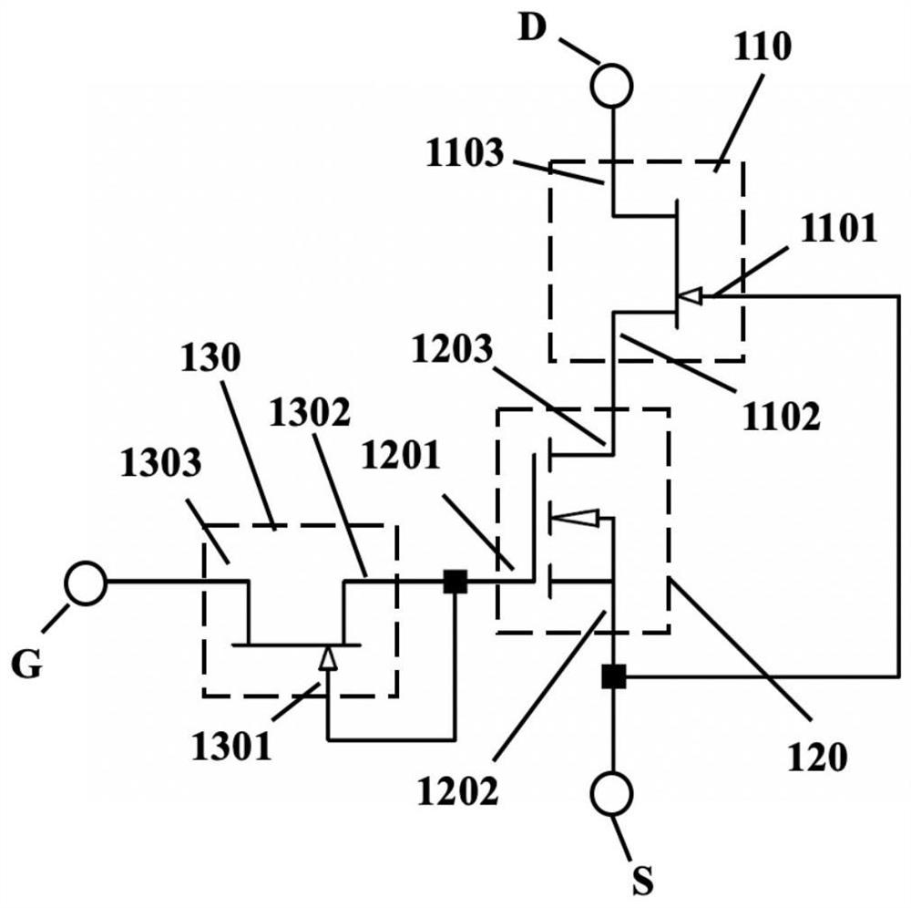
[0039] ginseng figure 1 As shown, a cascade circuit is disclosed in this embodiment, and the cascade circuit includes:

[0040] A high-voltage depletion device 110, a low-voltage enhancement device 120, and a low-voltage depletion device 130. The high-voltage depletion device 110 includes a first gate 1101, a first source 1102, and a first drain 1103. The low-voltage enhancement device 120 Including a second gate 1201 , a second source 1202 and a second drain 1203 , the low voltage depletion device 130 includes a third gate 1301 , a third source 1302 and a third drain 1303 . Wherein, the first source 1102 is electrically connected to the second drain 1203, the first gate 1101 is electrically connected to the second source 1202, and the second gate 1201 is electrically connected to the third source 1302 and the third gate 1301. The first drain 1103 serves as the drain D of the cascode circuit, the second source 1202 serves as the source S of the cascade circuit, and the third ...

Embodiment 2

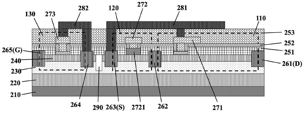
[0046] ginseng figure 2 As shown, a cascaded device is disclosed in this embodiment, and the cascaded device mainly includes a high voltage depletion device 110 , a low voltage enhanced device 120 and a low voltage depletion device 130 .

[0047] Specifically, the cascode device includes a substrate 210 , an epitaxial structure on the substrate, several passivation layers and several electrodes on the epitaxial structure.

[0048] Wherein, the epitaxial structure includes a channel layer 230 located on the substrate 210 and a barrier layer 240 located on the channel layer 230. Preferably, the epitaxial structure in this embodiment further includes a layer located between the channel layer 230 and the substrate 210. The buffer layer 220 between them.

[0049] Specifically, substrate 210 is one of silicon, sapphire, silicon carbide, etc.; buffer layer 220 is a combination of one or more of aluminum nitride layer, gallium nitride layer, aluminum gallium nitride layer, etc.; the...

Embodiment 3

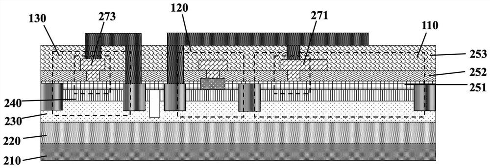
[0068] ginseng image 3 As shown, the cascaded device in this embodiment is similar to the cascaded structure in Embodiment 2, except for the high-voltage depletion device 110 and the low-voltage depletion device 130 .

[0069] In the high-voltage depletion-mode device 110 of this embodiment, the first gate 271 realizes the depletion-mode operation mode by a metal-insulator-semiconductor-based structure, and the first depletion region includes the entire second passivation layer 252 The first groove (not shown), the first grid 271 is partly located in the first groove, the first dielectric layer 251 is formed between the first grid 271 and the barrier layer 240, and the first dielectric layer 251 is used as a metal - insulating layer - an insulating layer in the structure of a semiconductor.

[0070] In the low-voltage depletion device 130 of this embodiment, the third gate 273 realizes the depletion mode of operation by a structure based on a metal-insulator-semiconductor, a...


PUM


Abstract

The invention discloses a cascaded circuit and cascaded device based on gate protection. The cascaded circuit includes a high-voltage depletion device, a low-voltage enhanced device, and a low-voltage depletion device. The high-voltage depletion device includes The first gate, the first source and the first drain, the low-voltage enhancement device includes the second gate, the second source and the second drain, the low-voltage depletion device includes the third gate, the third source and a third drain, the first source is electrically connected to the second drain, the first gate is electrically connected to the second source, the second gate is electrically connected to the third source and the third gate connected, the first drain serves as the drain of the cascode circuit, the second source serves as the source of the cascade circuit, and the third drain serves as the gate of the cascade circuit. The invention can greatly reduce the equivalent Miller capacitance of the traditional enhanced device, and even when the gate drive current is severely limited by the gate protection unit, the device can still meet the requirements for the switching speed of the device in practical applications.

Description

technical field [0001] The invention belongs to the technical field of semiconductors, and in particular relates to a gate protection-based cascaded circuit and a cascaded device. Background technique [0002] Gallium nitride, as a third-generation wide-bandgap semiconductor material, has excellent characteristics compared with traditional materials. First, GaN has a wide energy gap of 3.4eV and a high breakdown electric field exceeding 3MV / cm. Compared with silicon and gallium arsenide, the energy gap of more than 3 times and the breakdown electric field of more than 10 times make electronic devices based on gallium nitride have a higher withstand voltage and are more suitable for high-power applications. At the same time, similar to gallium arsenide, gallium nitride also has the ability to form a two-dimensional electron gas through a heterostructure. The difference is that in the AlGaN / GaN heterostructure, the two-dimensional electron gas can be naturally formed by the ...

Claims


Application Information

Patent Timeline
Patent Type & Authority Patents(China)
IPC IPC(8): H01L27/088
CPCH01L27/0883
Inventor 蒋胜柳永胜胡峰白强唐瑜陈辉于洁郑梦婕
Owner 苏州英嘉通半导体有限公司
Why Eureka
Try Eureka