Manufacturing method of meta-structure surface coupling element

A metasurface and coupling element technology, which is applied in the field of manufacturing metasurface coupling elements, can solve the problems of serious dispersion and processing difficulty, and achieve the effect of low processing difficulty

Active Publication Date: 2021-02-23
SHENZHEN LOCHN OPTICS HI-TECH CO LTD
View PDF6 Cites 3 Cited by
  • Summary
  • Abstract
  • Description
  • Claims
  • Application Information

AI Technical Summary

Problems solved by technology

[0004]However, for the design scheme of multi-layer color grating waveguide, there is often the problem of serious dispersion. In order to solve this prob...

Method used


Image

  • Manufacturing method of meta-structure surface coupling element
  • Manufacturing method of meta-structure surface coupling element
  • Manufacturing method of meta-structure surface coupling element

Examples


Embodiment Construction

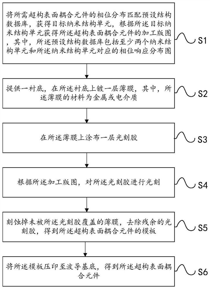
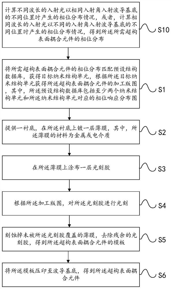
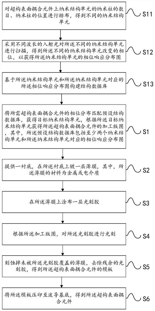
[0054] The present invention will be described in detail below in conjunction with specific embodiments. The following examples will help those skilled in the art to further understand the present invention, but do not limit the present invention in any form. It should be noted that those skilled in the art can make several modifications and improvements without departing from the concept of the present invention. These all belong to the protection scope of the present invention.

[0055]It should be noted that, if there is no conflict, various features in the embodiments of the present invention may be combined with each other, and all of them are within the protection scope of the present application. In addition, although the functional modules are divided in the schematic diagram of the device, and the logical order is shown in the flowchart, in some cases, the division of modules in the device or the sequence shown in the flowchart can be performed in different ways. or...


PUM

PropertyMeasurementUnit
Heightaaaaaaaaaa

Abstract

An embodiment of the invention relates to the technical field of optics, in particular to a manufacturing method of a meta-structure surface coupling element. The manufacturing method of the meta-structure surface coupling element provided by the embodiment of the invention comprises the following steps of: matching the phase distribution of a required meta-structure surface coupling element witha preset structure database to obtain a target nano-structure unit, and acquiring a processing layout of the meta-structure surface coupling element according to the target nano-structure unit, wherein the preset structure database comprises at least two nanostructure units and phase response distribution diagrams corresponding to the nanostructure units; providing a substrate, and plating a layerof metal or dielectric material film on the substrate; coating a layer of photoresist on the film; performing photoetching, etching and photoresist removing according to the processing layout to obtain a template of the meta-structure surface coupling element; and impressing the template to the waveguide substrate to obtain the meta-structure surface coupling element. The meta-structure surface coupling element manufactured through adopting the manufacturing method can be applied to an optical waveguide, achromatism can be achieved, and the machining difficulty is low.

Description

technical field [0001] The embodiments of the present invention relate to the field of optical technology, and in particular to a method for manufacturing a metasurface coupling element. Background technique [0002] At present, the relatively mature augmented reality technology is mainly divided into prism scheme, birdbath scheme, free-form surface scheme and waveguide scheme. The first three schemes are large in size, which limits their application in smart wear, and optical waveguide is currently the best Augmented reality glasses solution. [0003] The waveguide scheme is divided into geometric waveguide scheme, surface relief grating waveguide scheme and volume holographic waveguide scheme. The geometric waveguide solution uses an array of coated half-mirrors to display virtual information, but the field of view and eye movement range of this solution are limited, and the array lens will bring a stripe effect to the picture, so the geometric waveguide solution cannot g...

Claims


Application Information

Patent Timeline
IPC IPC(8): G02B6/136G02B6/13G02B6/122
CPCG02B6/136G02B6/13G02B6/122G02B2006/12176G02B2006/12166
Inventor 胡跃强姜玉婷张毅郭晓明段辉高宋强马国斌徐晓波
Owner SHENZHEN LOCHN OPTICS HI-TECH CO LTD
Why Eureka
Try Eureka