Mask plate, mask plate defect repairing method, mask plate using method and semiconductor structure

A defect repair and mask technology, applied in the field of semiconductor structure, can solve the problem of high cost, achieve high accuracy, improve repair rate and good performance

Pending Publication Date: 2021-02-23
SEMICON MFG INT (SHANGHAI) CORP +1
View PDF0 Cites 0 Cited by
  • Summary
  • Abstract
  • Description
  • Claims
  • Application Information

AI Technical Summary

Problems solved by technology

[0004] However, existing repair methods for mask defects are relatively expensive

Method used


Image

  • Mask plate, mask plate defect repairing method, mask plate using method and semiconductor structure
  • Mask plate, mask plate defect repairing method, mask plate using method and semiconductor structure
  • Mask plate, mask plate defect repairing method, mask plate using method and semiconductor structure

Examples


Embodiment Construction

[0028]As described in the context, the cost of existing mask version defects is high.

[0029]Figure 1 to 4 It is a structural diagram of a mask version of the lack of repair method.

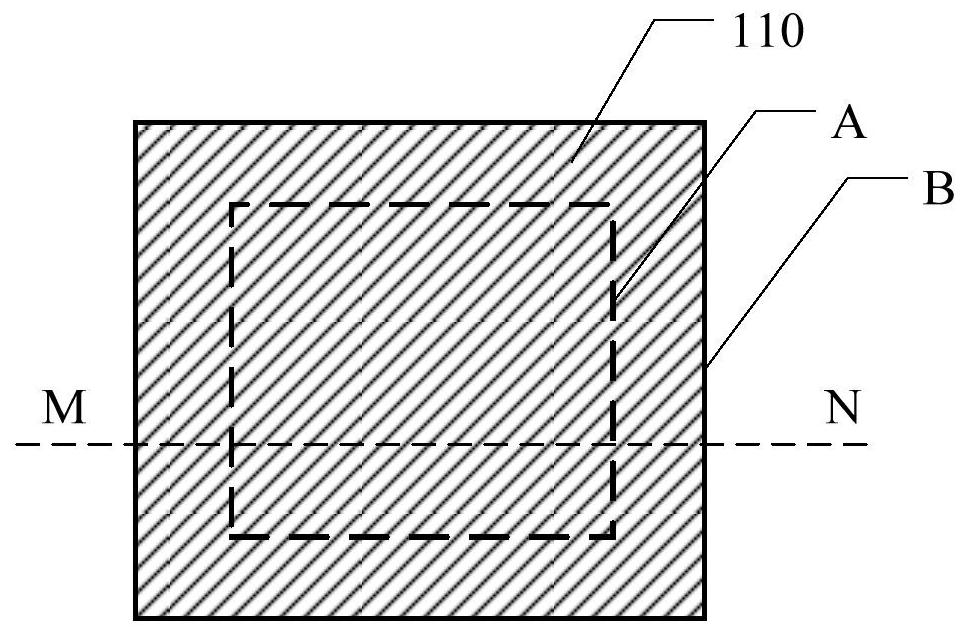
[0030]Please refer toFigure 1 to 2 ,figure 2 Yesfigure 1 A cross-sectional structure in the M-N tangent direction provides a substrate 100 that includes a region A region and a B region surrounding the A region, the substrate 100 having an initial light shielding layer 110.

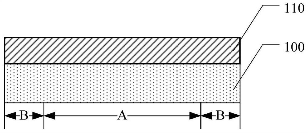
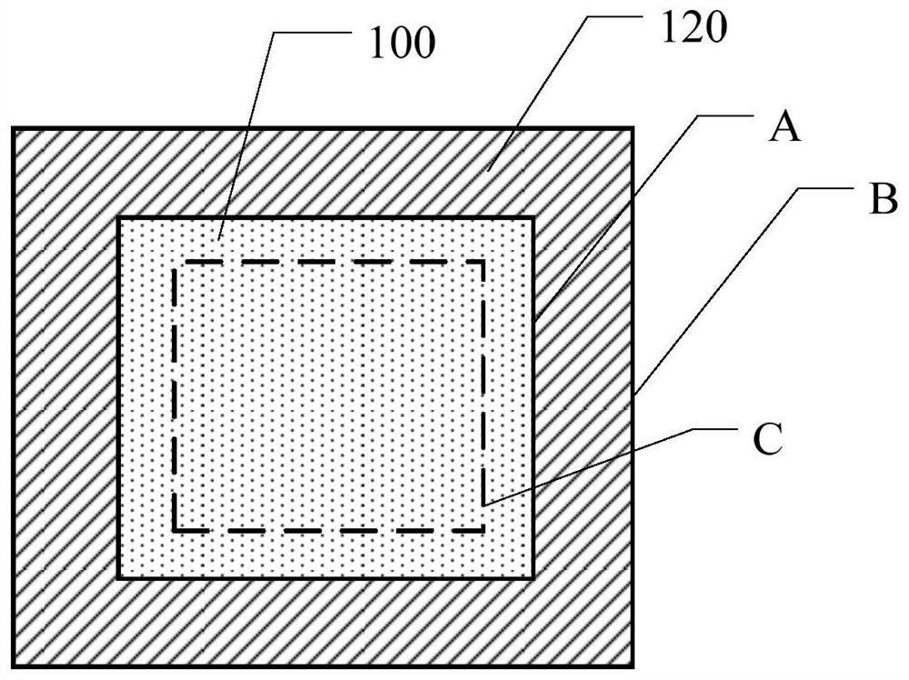
[0031]Please refer toFigure 3 to 4 ,image 3 Infigure 1 Based on the schematic,Figure 4 Infigure 2 Based on the schematic, the initial light shielding layer 110 is etched, and the light shielding layer 120 is formed on the B region, and the light shielding layer 120 has an opening 130, and the opening 130 is exposed to the surface of the A region.

[0032]In the above mask version of the lack of repair, the initial light shielding layer 110 is etched by an electron beam 140 mating gas to form a light shielding layer 120 and an opening 130 loc...


PUM


Abstract

The invention relates to a mask plate, a mask plate defect repairing method, a mask plate using method and a semiconductor structure; the mask plate defect repairing method comprises the following steps: providing a substrate, the substrate comprising a first area and a second area surrounding the first area, and the surface of the substrate being provided with a shading film; and performing morethan one time of first etching on the shading film to form a shading layer, the shading layer being internally provided with an opening, and the opening exposing the surface of the first region; the first etching comprises the following steps: forming a protective layer on the surface of the shading film; and performing a first electron beam etching process on the protective layer and the shadingfilm on the first region. According to the method, the etching deviation can be reduced and the mask defect repairing success rate can be improved while the mask defect repairing cost is reduced.

Description

Technical field[0001]The present invention relates to the field of semiconductor manufacturing, and more particularly to a mask plate, a mask release method, and a method of use, and a semiconductor structure.Background technique[0002]During the semiconductor manufacturing process, the photolithography process has always been a very important link, and the mask version is a pivotal position in photolithography. A common mask version includes a transparent substrate, for example, a quartz substrate, and a light shielding layer located on the substrate, typically the light shielding layer requires a metal. The mask version creates the pattern required in the semiconductor manufacturing process in the light shielding layer such that the pattern is formed on the silicon wafer through a series of processes.[0003]During the production process of the mask version, due to the various problems such as environmental, quartz substrates, a series of problems such as the pattern, photoresist, et...

Claims


Application Information

Patent Timeline
Patent Type & Authority Applications(China)
IPC IPC(8): G03F1/72G03F1/74
CPCG03F1/72G03F1/74
Inventor 秦学飞王杰薛粉凌文君李德建
Owner SEMICON MFG INT (SHANGHAI) CORP
Why Eureka
Try Eureka