
7T global shutter pixel structure based on semi-floating gate

A global shutter, pixel structure technology, applied in image communication, color TV components, TV system components and other directions, can solve the problems of small fill factor, large fill factor, low readout noise, etc., to achieve high global Shutter efficiency, high pixel fill factor, thermal noise removal effect

Active Publication Date: 2021-02-23
TIANJIN UNIV MARINE TECH RES INST
View PDF7 Cites 0 Cited by
  • Summary
  • Abstract
  • Description
  • Claims
  • Application Information

AI Technical Summary

Problems solved by technology

The first type of charge-domain global shutter pixel has a large fill factor, but the global shutter efficiency is low, and the readout noise is low and large, so it is not often used
The second and third types of charge domain global shutter pixels, although compared with the first type, KTC noise is completely eliminated, and the global shutter efficiency is greatly improved, but the fill factor is relatively small, and the process requirements are very high.
7T global shutter pixel fill factor is small, readout noise is large
[0004] At present, although the 8T pixel structure is the most commonly used, because the front part of the circuit structure is the same as the traditional 4T pixel structure, there is a problem that the voltage distribution between the photodetection area and the photoelectric conversion area in the traditional 4T pixel is difficult.

Method used


Image

  • 7T global shutter pixel structure based on semi-floating gate
  • 7T global shutter pixel structure based on semi-floating gate

Examples


Embodiment Construction

[0011] In order to further clarify the purpose, technical solutions and advantages of the present invention, specific implementations of the present invention are given below in conjunction with examples. In this instance:

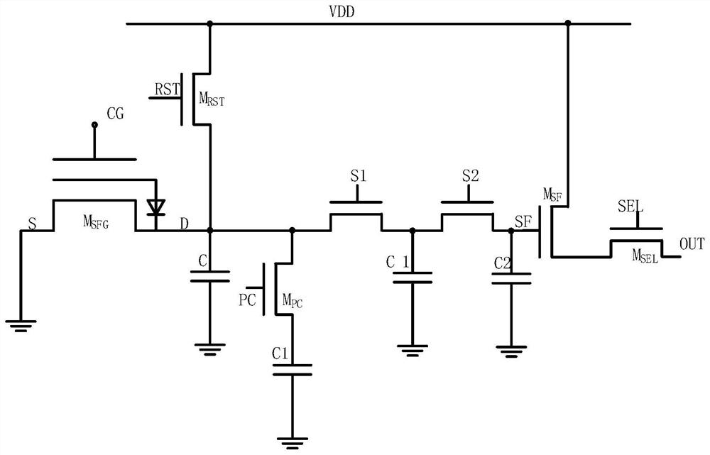
[0012] Semi-floating gate device M SFG Using NMOS tube, the width-to-length ratio is (1.2μm) / (6μm); the switch tube M PC Using NMOS tube, the width to length ratio is (4μm) / (5μm); reset tube M RST Using NMOS tube, the aspect ratio is (4μm) / (0.35μm); source follower M SF Using NMOS tube, the width to length ratio is (4μm) / (6μm); select tube M SEL Using NMOS tube, the width-to-length ratio is (4μm) / (5μm); the switch tube M S1 and M S2 They all use NMOS tubes with a width-to-length ratio of (4μm) / (5μm); capacitors C1 and C2 both use MOS capacitor structures with a capacitance value of 4fF.

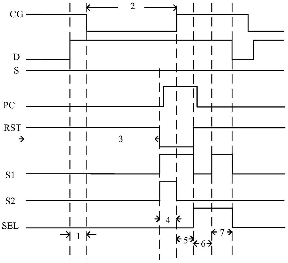
[0013] In timing design, the high level is 3.3V, and the low level is 0V. In the timing design part, the parameters of an exposure cycle are designed as follows: t...


PUM


Abstract

The invention discloses a 7T global shutter pixel structure based on a semi-floating gate. The 7T global shutter pixel structure comprises a semi-floating gate device MSFG, six switching tubes and twocapacitors, the structure comprises steps of firstly resetting a semi-floating gate MSFG, then exposing, finishing resetting a capacitor C during exposure, sampling and storing reset signals to capacitors C1 and C2, sampling and storing optical signals to the capacitor C1 after exposure is finished, and finally sequentially reading out the reset signals and the optical signals to finish a work cycle of the pixel structure provided by the invention. According to the structure, a problem of voltage distribution between a photoelectric detection region and a photoelectric conversion region of atraditional 8T pixel is solved, and compared with the 8T pixel, an MOS transistor is reduced, and a filling factor is increased.

Description

technical field [0001] The invention relates to the field of CMOS image sensors, in particular to a 7T global shutter pixel structure based on a half-floating gate. Background technique [0002] Since the invention of passive pixel image sensors in the 1960s, CMOS image sensors can be mainly divided into rolling shutter CMOS image sensors and global shutter CMOS image sensors according to different exposure methods. The difference between the rolling shutter CMOS image sensor and the global shutter CMOS image sensor is that the pixel array of the rolling shutter CMOS image sensor is exposed row by row, while the global shutter CMOS image sensor exposes the entire pixel array at the same time. When capturing fast-moving objects, the rolling shutter CMOS image sensor will cause a jelly effect due to the time difference in the exposure of each row of pixels, while the global shutter CMOS image sensor solves this drawback. The global shutter CMOS image sensor has become the bes...

Claims


Application Information

Patent Timeline
Patent Type & Authority Applications(China)
IPC IPC(8): H04N5/374H04N5/357
CPCH04N25/616H04N25/76Y02D10/00H04N25/771
Inventor 徐江涛李凤史兴萍王瑞硕夏梦真
Owner TIANJIN UNIV MARINE TECH RES INST
Learn More