Supercharge Your Innovation With Domain-Expert AI Agents!

Flaky resin composition for encapsulation and semiconductor device

A resin composition and sealing technology, used in semiconductor devices, semiconductor/solid-state device parts, electric solid-state devices, etc., can solve the problems of insufficient effect and low filling, and achieve improved formability and reduced wire flow effect

Active Publication Date: 2021-02-26
KYOCERA CORP
View PDF15 Cites 0 Cited by
  • Summary
  • Abstract
  • Description
  • Claims
  • Application Information

AI Technical Summary

Problems solved by technology

[0006] However, even if the sealing material used in the conventional transfer molding is applied to the compression molding method, the desired effect as described above cannot be sufficiently obtained due to its low filling property.

Method used


Image

  • Flaky resin composition for encapsulation and semiconductor device
  • Flaky resin composition for encapsulation and semiconductor device
  • Flaky resin composition for encapsulation and semiconductor device

Examples


Embodiment 1~7 and comparative example 1~4

[0096] The types and compounding amounts of the components listed in Table 1 were mixed using a mixer at normal temperature (25°C), and then heated and kneaded at 80 to 130°C using a hot roll. Under the condition of resin temperature of 60-110° C., rolls were used for rolling and cooling to obtain plates with thicknesses shown in Table 1.

[0097] The obtained board was pulverized using a high-speed pulverizer, and three types of JIS standard sieves (with a sieve diameter of 150 μm, 1 mm, and 2 mm) (JIS Z8801-1:2006 standard) were used to prepare resin compositions for sealing.

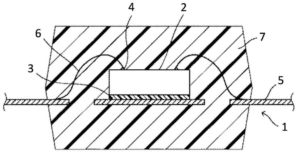
[0098] Moreover, sealing of a semiconductor chip was performed using the obtained resin composition for sealing. That is, using the resin composition for sealing, under the conditions of mold temperature of 175°C, molding pressure of 8.0MPa, and curing time of 2 minutes, a 50mm×50mm×0.54mm FBGA (Fine pitch Ball Grid Array, fine pitch ball grid array ) After compression molding, post-curing was perfor...


PUM

PropertyMeasurementUnit
thicknessaaaaaaaaaa
softening pointaaaaaaaaaa

Abstract

A flaky resin composition for encapsulation which comprises (A) an epoxy resin, (B) a phenolic-resin hardener, (C) a hardening accelerator, and (D) an inorganic filler, characterized in that 80 mass%or more of the flaky resin composition for encapsulation is accounted for by a flat-surface-containing resin composition which has a pair of flat parallel surfaces, the distance between the pair of flat surfaces being 150-1,000 [mu]m, and that the content of a flaky resin composition for encapsulation therein which, in classification with JIS standard sieves, passes through a sieve having a nominal opening size of 150 [mu]m is 5 mass% or less and the content of a flaky resin composition for encapsulation therein which, in said classification, does not pass through a sieve having a nominal opening size of 2 mm is 5 mass% or less.

Description

technical field [0001] The present invention relates to a sheet-like resin composition for semiconductor sealing and a semiconductor device. Background technique [0002] For sealing materials in semiconductor devices such as transistors, ICs (Integrated Circuits), and LSIs (Large Scale Integrations, large-scale integrated circuits), epoxy resins are mixed with curing agents and / or curing accelerators, and silica Resin composition of inorganic fillers such as powders, colorants, etc. [0003] Conventionally, the sealing process using such sealing materials is usually transfer molding. However, in recent years, along with the high-density mounting of electronic components on printed wiring boards, the mainstream of semiconductor devices has shifted from pin-insertion-type packages to surface-mount-type packages. In addition, surface mount packages are becoming thinner and smaller. In a thinner and smaller surface mount package, the volume occupied by the semiconductor elem...

Claims


Application Information

Patent Timeline
Patent Type & Authority Applications(China)
IPC IPC(8): C08L63/00C08G59/62C08K3/011C08K3/013H01L23/29H01L23/31
CPCC08G59/62C08K3/011C08K3/013C08L63/00H01L23/29H01L23/31H01L2924/181H01L2224/48247H01L2224/73265H01L2224/48465H01L2224/32245H01L2924/00012H01L2924/00C08G59/621C08L61/04H01L23/295
Inventor 须藤信博
Owner KYOCERA CORP
Features
  • R&D
  • Intellectual Property
  • Life Sciences
  • Materials
  • Tech Scout
  • Unparalleled Data Quality
  • Higher Quality Content
  • 60% Fewer Hallucinations
Learn More