Micro device facilitating picking and testing, manufacturing, testing and transferring method and display

A manufacturing method and micro-device technology, applied in semiconductor/solid-state device manufacturing, semiconductor/solid-state device testing/measurement, electric solid-state devices, etc., can solve problems such as inability to preliminarily screen LED core particles, reduce costs and improve utilization , the effect of avoiding pollution

Pending Publication Date: 2021-03-05
XIAMEN QIANZHAO SEMICON TECH CO LTD
View PDF1 Cites 2 Cited by
  • Summary
  • Abstract
  • Description
  • Claims
  • Application Information

AI Technical Summary

Problems solved by technology

[0005] The purpose of the present invention is to provide a pick-up and testable micro-device and a manufacturing, testing, transfer method and display to solve the problem that the prior art cannot realize the preliminary screening of LED chips before transfer in the process of manufacturing micro-device

Method used


Image

  • Micro device facilitating picking and testing, manufacturing, testing and transferring method and display
  • Micro device facilitating picking and testing, manufacturing, testing and transferring method and display
  • Micro device facilitating picking and testing, manufacturing, testing and transferring method and display

Examples


Embodiment Construction

[0074] In order to make the content of the present invention clearer, the content of the present invention will be further described below in conjunction with the accompanying drawings. The invention is not limited to this specific example. Based on the embodiments of the present invention, all other embodiments obtained by persons of ordinary skill in the art without making creative efforts belong to the protection scope of the present invention.

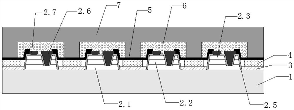
[0075] Such as figure 1 As shown, a micro device that can be picked up and tested includes:
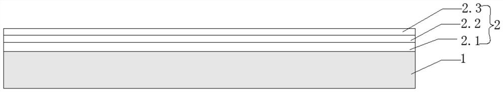
[0076] substrate1;

[0077] A plurality of LED chips arranged in an array on the surface of the substrate 1, two adjacent LED chips are separated from each other by grooves 2.4; each LED chip includes an epitaxial layer 2 and is located on the side of the epitaxial layer 2 facing away from the substrate 1 The first electrode 2.6 and the second electrode 2.7;

[0078] The first sacrificial layer 3, the first sacrificial layer 3 is forme...


PUM


Abstract

The invention provides a micro device facilitating picking and testing, a manufacturing, testing, transferring method and a display. A first sacrificial layer is arranged on the surface of a groove, and all testing electrodes are distributed above the first sacrificial layer corresponding to the groove at intervals and are far away from an LED core particle; the device also comprises multiple metal bridges, the metal bridges and the test electrodes are distributed in a crossed manner, the metal bridges are used for connecting the electrodes of two adjacent LED core particles in series, and themetal bridges are connected with the test electrodes at the corresponding grooves of the two adjacent LED core particles; the second sacrificial layer coats each LED core particle to form an independent coating unit; therefore, the integration of the LED core particles and the test structure is realized, and meanwhile, the purposes of arranging and sorting the LED core particles are achieved, sothat the perfect connection of subsequent test and transfer processes is ensured.

Description

technical field [0001] The invention relates to the field of light-emitting diodes, in particular to a pick-up and testable micro device, a manufacturing, testing and transferring method and a display. Background technique [0002] Micro-device technology refers to an array of micro-sized elements integrated at a high density on a substrate. At present, micro-pitch light-emitting diode (mini / micro LED) technology has gradually become a research hotspot, and the industry expects high-quality micro-device products to enter the market. High-quality fine-pitch light-emitting diode products will have a profound impact on traditional display products such as LCD / OLED that are already on the market. [0003] In existing LED chips, an automatic testing machine is generally used for spot testing, but the spot testing techniques in the prior art are generally applicable to LED chips of ordinary sizes. In the process of manufacturing micro-devices, due to the limited size of LED chip...

Claims


Application Information

Patent Timeline
Patent Type & Authority Applications(China)
IPC IPC(8): H01L27/15H01L21/66H01L21/67
CPCH01L21/67144H01L22/30H01L27/156
Inventor 谈江乔柯志杰艾国齐刘鉴明江方
Owner XIAMEN QIANZHAO SEMICON TECH CO LTD
Why Eureka
Try Eureka