Electromagnetic wave absorbing structure

An electromagnetic wave absorbing and resistive film technology, applied in electrical components, magnetic field/electric field shielding, antennas, etc., can solve the problems of high profile height, heavy weight, high density, etc., and achieve the effect of low profile and low cost

Pending Publication Date: 2021-03-05
唐明春
View PDF7 Cites 1 Cited by
  • Summary
  • Abstract
  • Description
  • Claims
  • Application Information

AI Technical Summary

Problems solved by technology

The coating-type absorbing structure often uses magnetic materials such as ferrite and metal micropowder as the absorber, which has the advantages of small thickness and wide absorbing frequency band, but it has high density and heavy mass.
Pyramids and multi-layer boards made of structural absorbing materials filled with foam and sponge have the advantages of high absorption efficiency, light weight, and absorption bandwidth, but their section height is large

Method used


Image

  • Electromagnetic wave absorbing structure
  • Electromagnetic wave absorbing structure
  • Electromagnetic wave absorbing structure

Examples


Embodiment 1

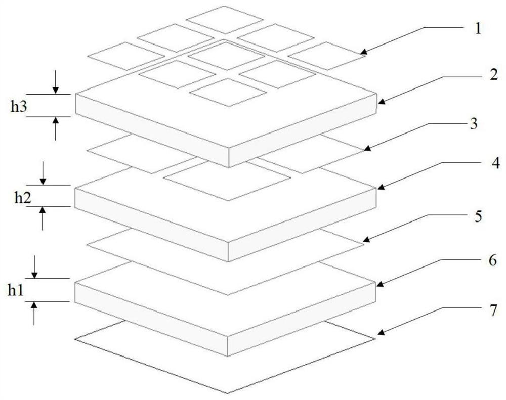
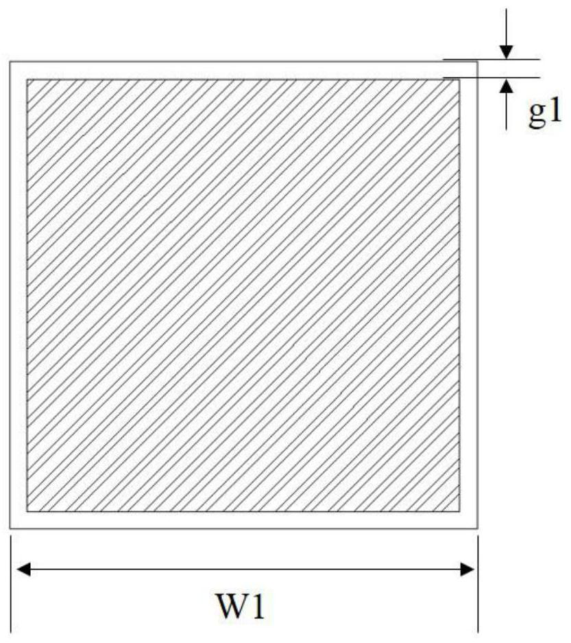
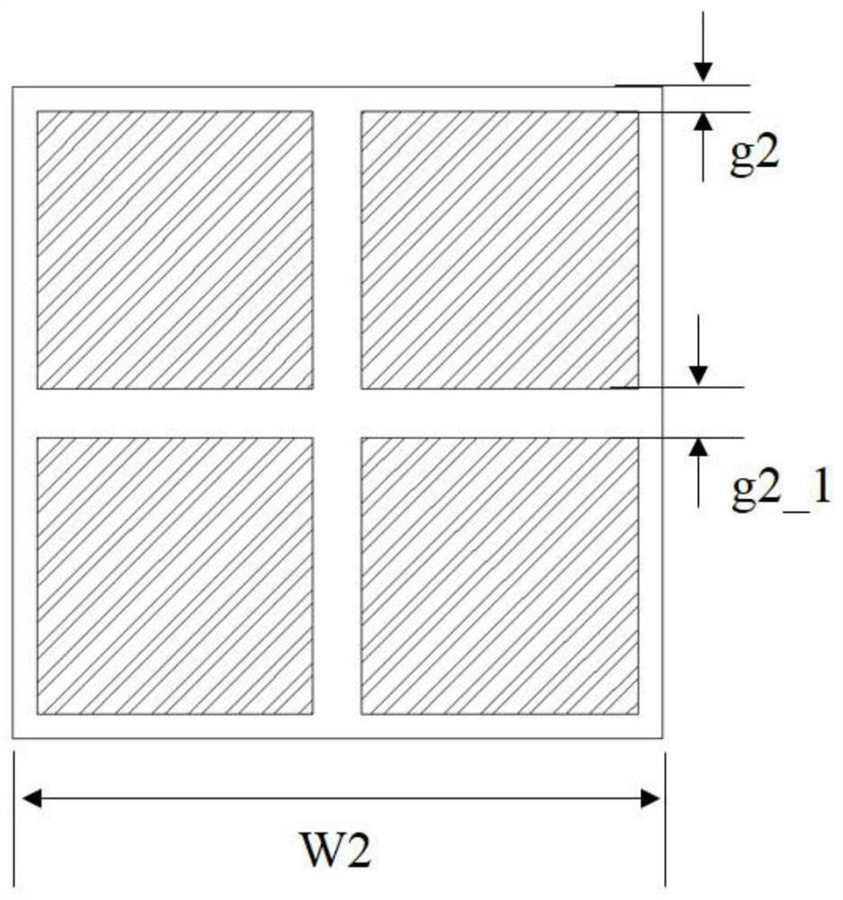
[0043] When the three-layer film unit is 1:2 2 :3 2 When setting the resistance film, its specific size parameters are (s unit: mm): W1=W2=W3=250mm, g1=g2=g3=14mm, g1_1=g2_1=g2_2=g3_1=g3_2=g3_3=28mm, h1=h2 =h3=40mm. The square resistance of the first film unit is s1=90ohm / sq, the square resistance of the second film unit is s2=210ohm / sq, and the square resistance of the third film unit is s3=255ohm / sq. In the case of vertically incident TE or TM waves, this embodiment has Figure 7 The absorbing performance shown. It has a reflection coefficient below -10dB in the entire frequency band of 0.3-3GHz, among which, the entire frequency band of 0.4-2GHz has a reflection coefficient of below -15dB, and the profile height is 0.12λ 0 .

Embodiment 2

[0045] When the three-layer film unit is 1:2 2 :3 2 When setting the resistance film, its specific size parameters are (s unit: mm): W1=W2=W3=80mm, g1=g2=g3=3mm, g1_1=g2_1=g2_2=6mm, h1=h2=h3=8mm. The square resistance s1 of the first film unit is 120 ohm / sq, the square resistance s2 of the second film unit is 190 ohm / sq, and the square resistance s3 of the third film unit is 377 ohm / sq. In the case of vertically incident TE or TM waves, this embodiment has Figure 6 The absorbing performance shown. It has a reflection coefficient below -10dB in the entire frequency band of 1.2-14GHz, and the profile height is 0.1λ 0 .

Embodiment 3

[0047] When the four-layer film unit is 1:2 2 :3 2 :4 2 When setting the resistance film, its specific size parameter is (s unit: mm): W1=W2=W3=W4=25mm, g1=g2=g3=g4=0.5mm, g1_1=g2_1=g3_1=g3_2=g4_1=g4_2= g4_3=1mm, h1=h2=h3=h4=4mm. The square resistance of the first layer of thin film unit s1=90ohm / sq, the square resistance of the second layer of thin film unit s2=210ohm / sq, the square resistance of the third layer of thin film unit s4=350ohm / sq, the square resistance of the fourth layer of thin film unit s4 = 377 ohm / sq. In the case of vertically incident TE or TM waves, this embodiment has Figure 8 The absorbing performance shown. It has a reflection coefficient of about -20dB in the entire frequency band of 2.5-38GHz, and the profile height is 0.14λ 0 .


PUM


Abstract

The invention relates to an electromagnetic wave absorbing structure which comprises a metal floor and k layers of wave absorbing modules sequentially arranged on the metal floor. The ith layer of wave absorbing module comprises an ith layer of foam substrate and an ith layer of thin film unit, and the ith layer of thin film unit is arranged on the ith layer of foam substrate; the ith layer of thin film unit comprises p2 * m * n resistive thin films which are arranged on the ith layer of foam substrate in an array manner; the (i + 1) th layer of thin film unit comprises q2 * m * n resistive thin films which are arranged on the (i + 1) th layer of foam substrate in an array mode, q is larger than p, and q and p are both positive integers larger than or equal to 1. The electromagnetic wave-absorbing structure disclosed by the invention can simultaneously meet the requirements of low cost, light weight, low profile and high-efficiency ultra-wideband wave absorption, realizes high-efficiency wave absorption within 10 octave ranges at the profile height of 0.08-0.15[lambda]0 initial working frequency, has the absorptivity of more than 90%, and can effectively cover 30-300MHz, 300MHz 3GHz frequency bands or 3-30GHz and other ultra-wide frequency bands.

Description

technical field [0001] The invention relates to the technical field of electronic materials, in particular to an electromagnetic wave-absorbing structure. Background technique [0002] The absorbing structure refers to the structure that can effectively absorb the incident electromagnetic wave and make it scatter and attenuate. Different absorbing structure design methods can achieve different electromagnetic wave losses, but the purpose is to reduce the number of interfering electromagnetic waves. The design goal is to "Thin, light, wide and strong", that is, the thickness of the absorbing structure is thinner, the weight is lighter, the absorbing band is wider, and the absorbing effect is stronger. The coating-type absorbing structure often uses magnetic materials such as ferrite and metal micropowder as the absorber, which has the advantages of small thickness and wide absorbing frequency band, but it has high density and heavy mass. Pyramids and multi-layer boards made ...

Claims


Application Information

Patent Timeline
Patent Type & Authority Applications(China)
IPC IPC(8): H01Q17/00H05K9/00
CPCH01Q17/00H05K9/0088
Inventor 石婷唐明春
Owner 唐明春
Why Eureka
Try Eureka