Semiconductor wafer surface cleaning device

A surface cleaning and semiconductor technology, which is applied to cleaning methods using liquids, cleaning methods and utensils, cleaning methods using tools, etc., which can solve the problems of consuming more manpower and time, easy residual impurities on the wafer surface, and outdated cleaning methods, etc. problems, to achieve the effect of improving practicability and reliability

Active Publication Date: 2021-03-12
浙江汇隆晶片技术有限公司
View PDF8 Cites 1 Cited by
  • Summary
  • Abstract
  • Description
  • Claims
  • Application Information

AI Technical Summary

Problems solved by technology

[0002] As we all know, a semiconductor wafer is mainly an electronic auxiliary component composed of silicon, which is usually a thin sheet. When the wafer is processed and produced with electronic components, it is necessary to clean up the impurities attached or remaining on the surface of the wafer, so as to ensure The cleanliness of the wafer surface prevents impurities from polluting and damaging the electronic components. The existing cleaning method is mainly for workers to clean the surface of the wafer with a brush. The cleaning method is relatively old and requires a lot of manpower and time. At the same time, after manual cleaning Impurities are easy to remain on the surface of the wafer, resulting in poor cleaning effect

Method used


Image

  • Semiconductor wafer surface cleaning device
  • Semiconductor wafer surface cleaning device
  • Semiconductor wafer surface cleaning device

Examples


Embodiment Construction

[0019] The specific implementation manners of the present invention will be further described in detail below in conjunction with the accompanying drawings and embodiments. The following examples are used to illustrate the present invention, but are not intended to limit the scope of the present invention.

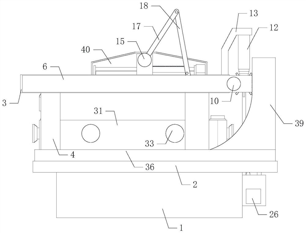
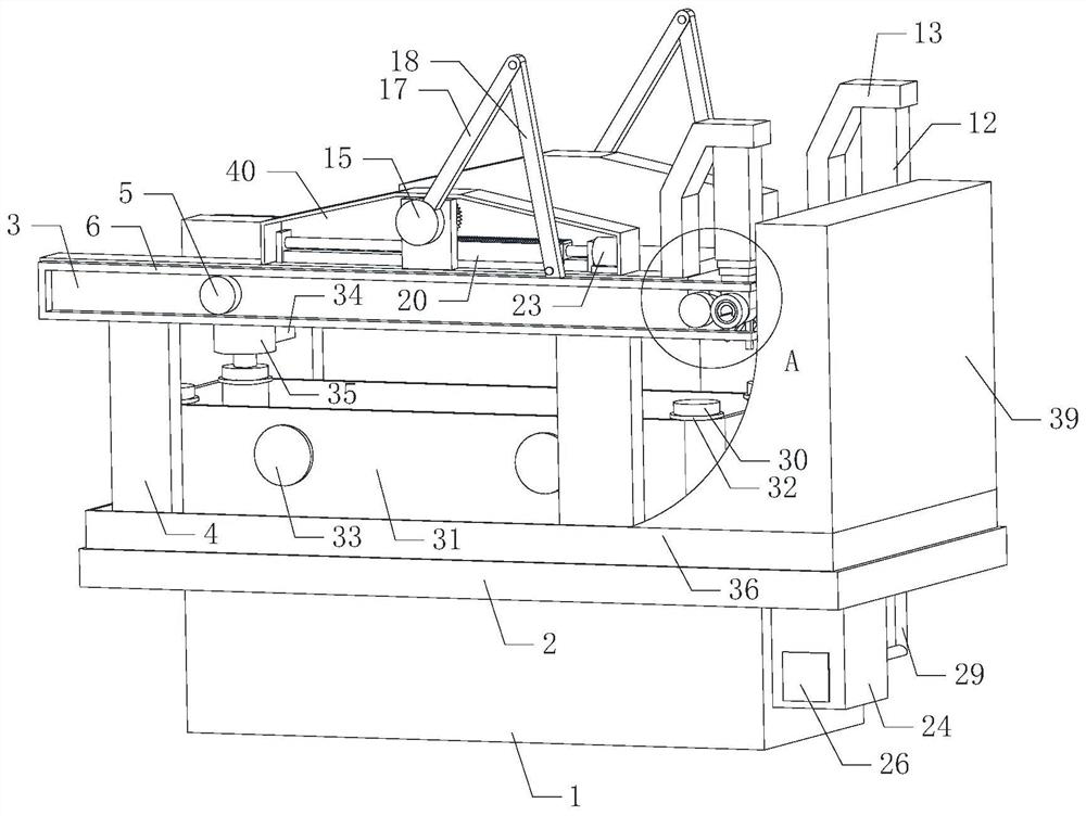
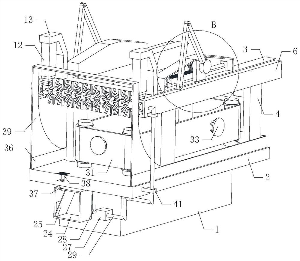
[0020] Such as Figure 1 to Figure 5 As shown, a semiconductor wafer surface cleaning device of the present invention, when it is working, opens two groups of second motors 23, and the two groups of second motors 23 drive the rolling resistance screw 22 to rotate, and the two groups of screw screws 22 are respectively connected to The two sets of sliders 20 are screw-mounted and connected, and the two sets of lead screws 22 synchronously push the two sets of sliders 20 to move left and right. The two sets of sliders 20 slide on the two sets of guide rails 19 respectively. Engage with the bottoms of the two groups of gears 16 respectively, the two groups of sliders 20 resp...


PUM


Abstract

The invention relates to the technical field of mechanical equipment, in particular to a semiconductor wafer surface cleaning device which can conveniently improve the cleanliness of the surface of awafer, improve the cleaning effect, reduce impurity residues, save the physical strength and time during manual cleaning, improve the working efficiency and improve practicability and reliability by automatically cleaning the wafer. The semiconductor wafer surface cleaning device comprises a base, a workbench, a U-shaped frame, four sets of supporting legs, two sets of tugs and two sets of supporting groove plates, wherein a water supply device is arranged on the right side of the base, the workbench is installed on the base, a feeding device is transversely arranged at the top of the workbench, the U-shaped frame is located above the workbench and fixed to the outer side of the top of the workbench through the four sets of supporting legs, and the two sets of tugs are rotationally installed on the left side of the front portion and the left side of the rear portion of the U-shaped frame respectively.

Description

technical field [0001] The invention relates to the technical field of mechanical equipment, in particular to a semiconductor wafer surface cleaning device. Background technique [0002] As we all know, a semiconductor wafer is mainly an electronic auxiliary component composed of silicon, which is usually a thin sheet. When the wafer is processed and produced for electronic components, it is necessary to clean up the impurities attached or remaining on the wafer surface, so as to ensure The cleanliness of the wafer surface prevents impurities from polluting and damaging the electronic components. The existing cleaning method is mainly for workers to clean the surface of the wafer with a brush. The cleaning method is relatively old and requires more manpower and time. At the same time, after manual cleaning Impurities tend to remain on the surface of the wafer, resulting in poor cleaning effect. Contents of the invention [0003] In order to solve the above-mentioned techn...

Claims


Application Information

Patent Timeline
Patent Type & Authority Applications(China)
IPC IPC(8): B08B1/00B08B1/04B08B3/02B08B13/00
CPCB08B1/008B08B1/04B08B3/024B08B13/00
Inventor 吴禹凡高洪庆
Owner 浙江汇隆晶片技术有限公司
Why Eureka
Try Eureka