Display panel

A display panel and display area technology, which is applied in the direction of static indicators, instruments, electrical components, etc., can solve the problems of poor taste of low gray scale, low reset voltage, slow anode lighting, etc., to achieve uniform brightness, reduced impedance, The effect of pressure drop reduction

Pending Publication Date: 2021-03-12
WUHAN CHINA STAR OPTOELECTRONICS SEMICON DISPLAY TECH CO LTD
View PDF9 Cites 1 Cited by
  • Summary
  • Abstract
  • Description
  • Claims
  • Application Information

AI Technical Summary

Problems solved by technology

[0002] Active-matrix organic light-emitting diode (AMOLED), due to its relatively complex circuit structure, has the advantages of wide viewing angle, ultra-high contrast, low power consumption, and fast response. And equipment and other factors make its micro-uniformity insufficient
In particular, the uneven characteristics of the thin film transistor (TFT) of the PMOS (n-type substrate, p-channel, MOS tube that relies on the flow of holes to carry current) devices will lead to uneven brightness of the AMOLED display under low light conditions (mura ) and color shift
[0003] For some high-end display panels, consumers prefer narrow bezels and full-screen designs. The current high-end mobile phones all adopt the structure of setting cameras under the panel (camera under panel), such as figure 1 As shown, this leads to difficulty in the design of the dense structure near the imaging hole 11. Generally, the reset line 12 near the imaging hole 11 connects each row of sub-pixels, and each row of sub-pixels is disconnected near the imaging hole 11 through the reset line 12 near the imaging hole 11. The oval line is connected, and the up and down sub-pixels are not connected in parallel. The reset capability of the reset line 12 near the camera hole 11 is stronger than that of the display area, and the reset voltage of the anode line is lower. The panel shows that the anode of the AMOLED is slow to light up, and the brightness of the display is uneven near the camera hole 11 when the screen is displayed.

Method used


Image

  • Display panel
  • Display panel
  • Display panel

Examples


Embodiment 3

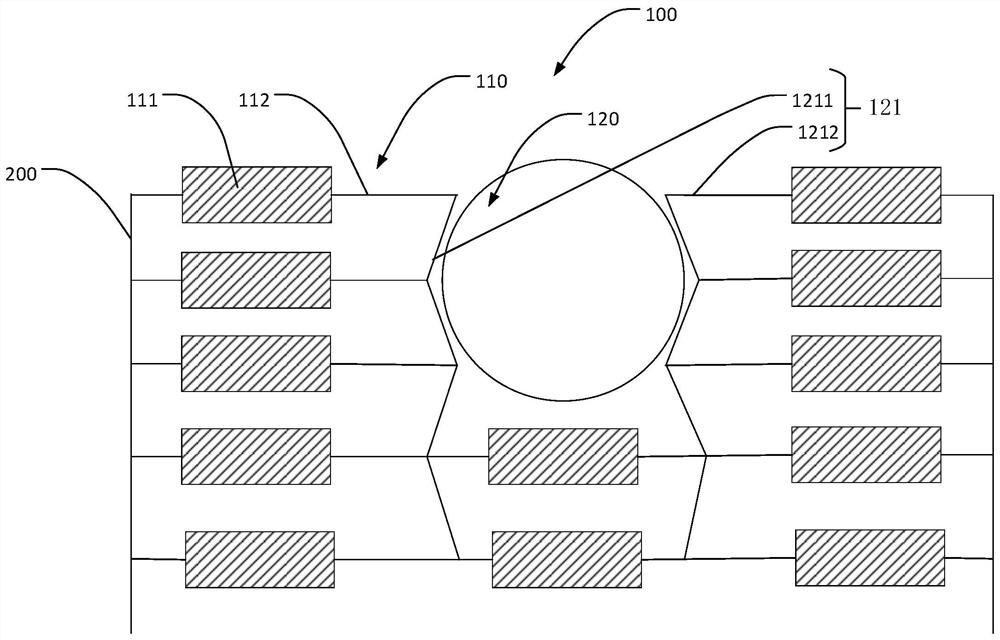
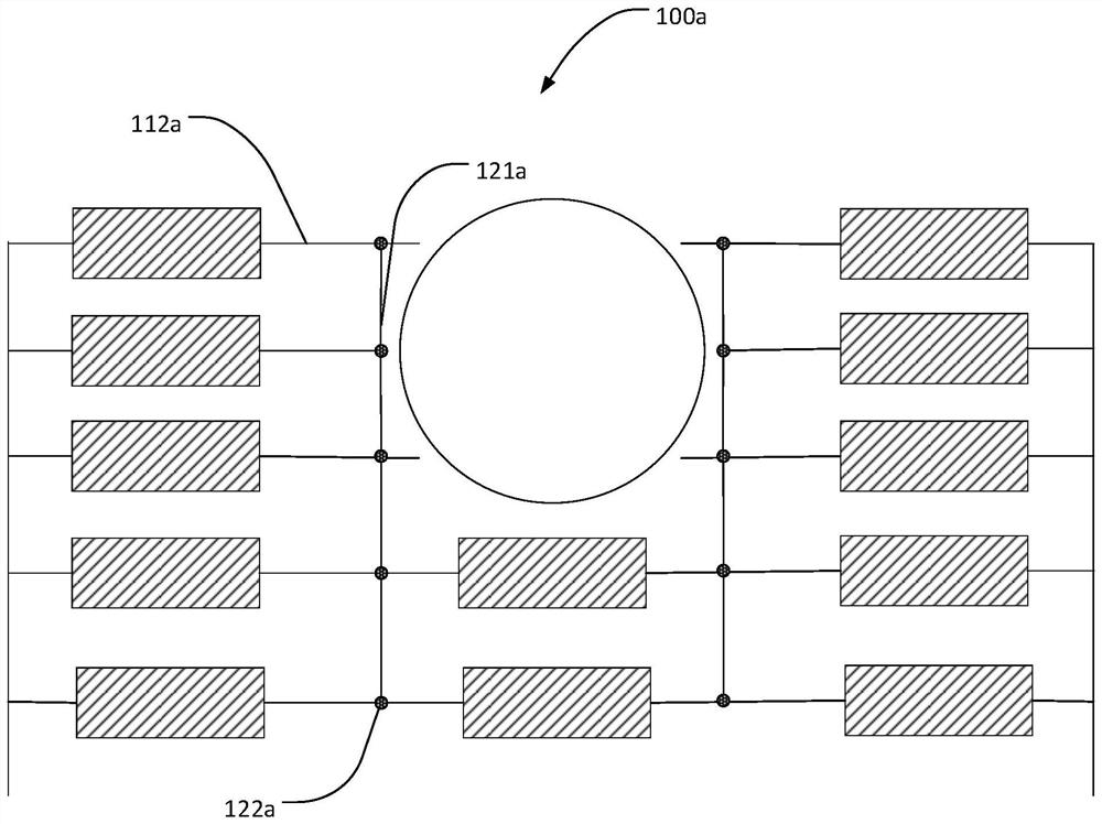
[0061] The connection manner of the second connection line 121b and the first connection line 112b in Embodiment 3 can also be connected through the through hole 122b, that is, the second connection line 121b and the first connection line 112b can also be arranged in different layers.

[0062] In addition, the left connection line 1211b and the right connection line 1212b in Embodiment 3 can also be directly connected, which increases the stability of the circuit structure.

[0063] The number of the left connection wire 1211b and the right connection wire 1212b in Embodiment 3 is at least two, which is used to increase the stability of the circuit structure, and when one of them is disconnected, the other one can still function as a connection role.


PUM


Abstract

The invention provides a display panel. The display panel comprises a light-transmitting area, a display area, a reset signal line, a first connecting line and a second connecting line. According to the invention, the sub-pixels in the two adjacent rows are connected in parallel, so that the impedance between the pixels is reduced, the voltage on the panel is closer, and the voltage drop on the panel can be reduced. When part of the first connecting lines at the light-transmitting area are disconnected, part of the disconnected rows of sub-pixels of the part of the first connecting lines are indirectly connected through the second connecting lines, then indirect connection of the first connecting lines corresponding to the light-transmitting area is achieved, and the rows of sub-pixels corresponding to the light-transmitting area are connected in parallel, so that the voltage of the whole reset signal in the light-transmitting area is kept consistent, the brightness of the display nearthe light-transmitting area is uniform, and the grade of the panel is improved.

Description

technical field [0001] The invention relates to the field of flexible displays, in particular to a display panel. Background technique [0002] Active-matrix organic light-emitting diode (AMOLED), due to its relatively complex circuit architecture, it has the advantages of wide viewing angle, ultra-high contrast, low power consumption, and fast response. And equipment and other factors make its micro-uniformity insufficient. In particular, the uneven characteristics of the thin film transistor (TFT) of the PMOS (n-type substrate, p-channel, MOS tube that relies on the flow of holes to carry current) devices will lead to uneven brightness of the AMOLED display under low light conditions (mura ) and color shift. [0003] For some high-end display panels, consumers prefer narrow bezels and full-screen designs. Currently, high-end mobile phones use a camera under panel structure (camera under panel), such as figure 1 As shown, this leads to the difficulty in the design of the...

Claims


Application Information

Patent Timeline
Patent Type & Authority Applications(China)
IPC IPC(8): H01L27/32G09G3/3225
CPCG09G3/3225G09G2320/0233H10K59/122H10K59/123H10K59/1315H10K59/1213
Inventor 胡凯苏博宇
Owner WUHAN CHINA STAR OPTOELECTRONICS SEMICON DISPLAY TECH CO LTD
Why Eureka
Try Eureka