Check patentability & draft patents in minutes with Patsnap Eureka AI!

Static random access memory device

A static random access, memory cell technology, applied in static memory, digital memory information, information storage, etc., can solve problems such as write failure, read interference, and reduction

Pending Publication Date: 2021-03-19
UNITED MICROELECTRONICS CORP
View PDF0 Cites 0 Cited by
  • Summary
  • Abstract
  • Description
  • Claims
  • Application Information

AI Technical Summary

Problems solved by technology

The traditional 6T-SRAM memory cell uses the same access transistor to control the read of the same storage node, and the read static noise margin (read static noise margin, SNM) and the write margin (write margin) are both reduced during low-voltage operation. , coupled with the drift of the process, it is prone to problems such as half-select disturbance, (half-select disturbance), read disturbance (read disturbance) and write failure (write failure)

Method used


Image

  • Static random access memory device
  • Static random access memory device
  • Static random access memory device

Examples


Embodiment Construction

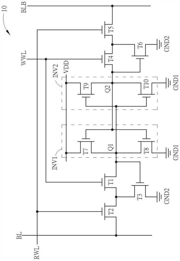
[0019] figure 1 It is a schematic diagram of a ten-transistor SRAM (ten-transistor SRAM, 10T-SRAM) memory unit 10 in an embodiment of the present invention. The 10T-SRAM memory cell 10 includes transistors T1 - T10 , and each transistor can control a signal conduction path between its first terminal and its second terminal according to the potential of its control terminal. In the embodiment of the present invention, the transistors T1-T10 may be implemented by metal-oxide-semiconductor field-effect transistors (MOSFET) or bipolar junction transistors (bipolar junction transistor, BJT). However, the transistors The implementation manners of T1-T10 do not limit the scope of the present invention.

[0020] A first terminal of the access transistor T1 is coupled to the storage node Q1, and a control terminal is coupled to the word line WWL. The first terminal of the access transistor T2 is coupled to the second terminal of the access transistor T1, the second terminal is couple...


PUM


Abstract

A static random access memory device includes two inverters and first to third transistors. A first end of the first inverter is coupled to a first data node, and a second end of the first inverter iscoupled to a second data node. The first end of the second inverter is coupled to the second data node, and the second end is coupled to the first data node. The first transistor includes a first terminal, a second terminal, and a control terminal coupled to a first data node. The second transistor includes a first terminal coupled to the second terminal of the first transistor, a second terminalcoupled to the first bit line, and a control terminal. The third transistor includes a first terminal coupled between the second terminal of the first transistor and the first terminal of the secondtransistor, a second terminal, and a control terminal coupled to the first data node.

Description

technical field [0001] The invention relates to a static random access memory device, in particular to a static random access memory device with a holding circuit. Background technique [0002] An embedded static random access memory (embedded SRAM) includes a logic circuit and the SRAM connected to the logic circuit. The SRAM itself is a volatile memory cell (memory cell), that is, when the power supplied to the SRAM disappears, the stored data will be erased at the same time. Static random access memory stores data by using the conductive state of transistors in memory cells. The design of static random access memory is based on mutual coupling transistors. There is no problem of capacitor discharge, and it does not need to be continuously charged to keep data. Drain, that is, the action of not needing to update the memory, is different from that of the dynamic random access memory (DRAM), which is also a volatile memory, by using the charged state of the capacitor to sto...

Claims


Application Information

Patent Timeline
Patent Type & Authority Applications(China)
IPC IPC(8): G11C11/412H10B10/00
CPCG11C11/412G11C8/16G11C11/4125G11C7/02H10B10/12G11C11/419H10B10/00
Inventor 邱子育陈信彣莫亚楠陈元辉蔡忠政
Owner UNITED MICROELECTRONICS CORP
Features
  • R&D
  • Intellectual Property
  • Life Sciences
  • Materials
  • Tech Scout
  • Unparalleled Data Quality
  • Higher Quality Content
  • 60% Fewer Hallucinations
Learn More