Hot-pressing bonding method of high-frequency circuit board and processing method of circuit board

A high-frequency circuit board and bonding method technology, applied in high-frequency matchers, laminated printed circuit boards, printed circuits, etc., can solve the problems of decreased reliability of circuit boards, insufficient bonding force between boards, and cracked board plating. , to achieve the effect of increasing surface area, improving adhesion, and large contact area

Active Publication Date: 2021-03-19
HUIZHOU TECHUANG ELECTRONIC TECH CO LTD
View PDF8 Cites 0 Cited by
  • Summary
  • Abstract
  • Description
  • Claims
  • Application Information

AI Technical Summary

Problems solved by technology

[0003] When the multi-layer Teflon circuit board is pressed, the effects of crystal extension, diffusion and bonding between the cured sheet and the Teflon board are very weak, mainly relying on mechanical bonding, so the surface structure of the Teflon board has a great influence on the bonding effect. The impact is more prominent. It is necessary to improve the surface structure of the Teflon plate through roughening to improve the bonding force. The Teflon material has good physical and chemical properties, and it is difficult to react with the roughening potion. Therefore, the potion is used for Teflon. The surface roughening of the dragon board can only achieve a meager roughening effect. After the Teflon board body is pressed to form a multi-layer board, there will often be insufficient bonding between the boards, which will lead to the explosion of the board or the peeling off of the coating. The reliability of the circuit board is reduced

Method used


Image

  • Hot-pressing bonding method of high-frequency circuit board and processing method of circuit board

Examples


Embodiment Construction

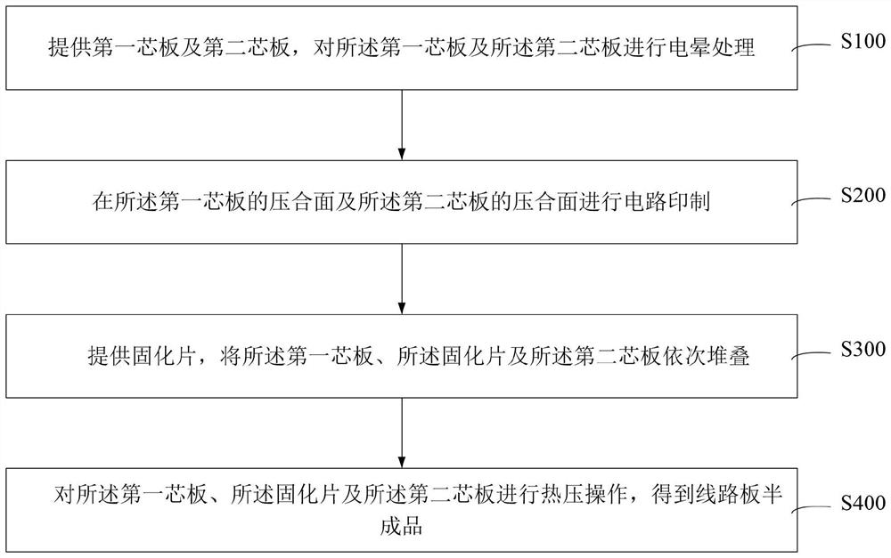
[0032] In order to facilitate the understanding of the present invention, the present invention will be described more fully below with reference to the associated drawings. Preferred embodiments of the invention are shown in the accompanying drawings. However, the present invention can be embodied in many different forms and is not limited to the embodiments described herein. On the contrary, the purpose of providing these embodiments is to make the disclosure of the present invention more thorough and comprehensive.

[0033] It should be noted that when an element is referred to as being “fixed” to another element, it can be directly on the other element or there can also be an intervening element. When an element is referred to as being "connected to" another element, it can be directly connected to the other element or intervening elements may also be present. The terms "vertical," "horizontal," "left," "right," and similar expressions are used herein for purposes of ill...


PUM


Abstract

The invention provides a hot-pressing bonding method of a high-frequency circuit board and a processing method of the circuit board. The hot-pressing bonding method of the high-frequency circuit boardcomprises the following steps: providing the first core board and the second core board, and carrying out corona treatment on the first core board and the second core board; performing circuit printing on the pressing surface of the first core plate and the pressing surface of the second core plate; providing a curing sheet, and sequentially stacking the first core plate, the curing sheet and thesecond core plate; and carrying out hot pressing operation on the first core plate, the curing sheet and the second core plate. The lamination surfaces of the first core plate and the second core plate are subjected to corona surface treatment, and countless grooves and micropores are formed in the lamination surfaces, so that the surface area of the lamination surfaces can be increased, the lamination surfaces and the cured sheet have a larger contact area, and the bonding force between the lamination surfaces and the cured sheet is increased; meanwhile, the curing sheet is embedded into thegroove or the micropore of the pressing surface under the action of pressure, and the curing sheet and the groove or the micropore form lock catch connection, so that the situation that the plate isexploded due to insufficient binding force of the plate is effectively prevented.

Description

technical field [0001] The invention relates to the technical field of circuit board processing, in particular to a thermocompression bonding method for a high-frequency circuit board and a processing method for the circuit board. Background technique [0002] With the rapid development of the world's communication industry, various electronic consumer products with high-speed information processing functions have become an indispensable part of people's daily life. The development speed of the transfer from the military field to civilian consumption. Since the dielectric constant and dielectric loss factor of Teflon materials are low, and the dielectric constant and dielectric loss factor of Teflon materials are stable at different frequencies, Teflon materials with excellent high-frequency characteristics and high reliability are used It is widely used in high-frequency circuit boards. [0003] When the multi-layer Teflon circuit board is pressed, the effects of crystal ...

Claims


Application Information

Patent Timeline
Patent Type & Authority Applications(China)
IPC IPC(8): H05K1/02H05K3/00
CPCH05K1/0237H05K3/0058
Inventor 许校彬陈金星肖尊民
Owner HUIZHOU TECHUANG ELECTRONIC TECH CO LTD
Why Eureka
Try Eureka