Micro-cavity with chiral polarization selectivity as well as preparation method and application thereof
A selective and polarized technology, applied in optical components, optics, instruments, etc., can solve the problems of increasing the complexity of the optical path, difficult to achieve the simplicity of device integration and testing, reducing the dependence on external conditions, simplifying the optical path, The effect of improving simplicity
- Summary
- Abstract
- Description
- Claims
- Application Information
AI Technical Summary
Problems solved by technology
Method used
Image


Examples
Embodiment 1
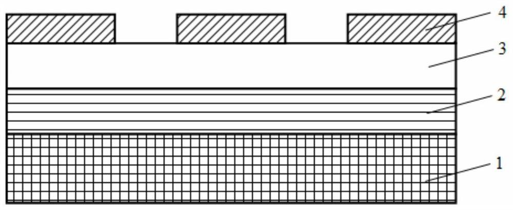
[0025] A microcavity with chiral polarization selectivity, such as figure 1 As shown, a substrate 1 , a metal mirror 2 , a dielectric layer 3 and a chiral metamaterial 4 are sequentially included from bottom to top. The preparation of the microcavity with chiral polarization selectivity comprises the following steps:
[0026] In the first step, a metal mirror 2 with high reflectivity is plated on the substrate 1 by electron beam evaporation technology; wherein, the material used for the substrate 1 is silicon, and the material used for the metal mirror 2 is silver, with a thickness of 800nm.
[0027] In the second step, a dielectric layer 3 is plated on the metal mirror 2 by electron beam evaporation technology; wherein, the material used for the dielectric layer 3 is silicon oxide with a thickness of 233nm.
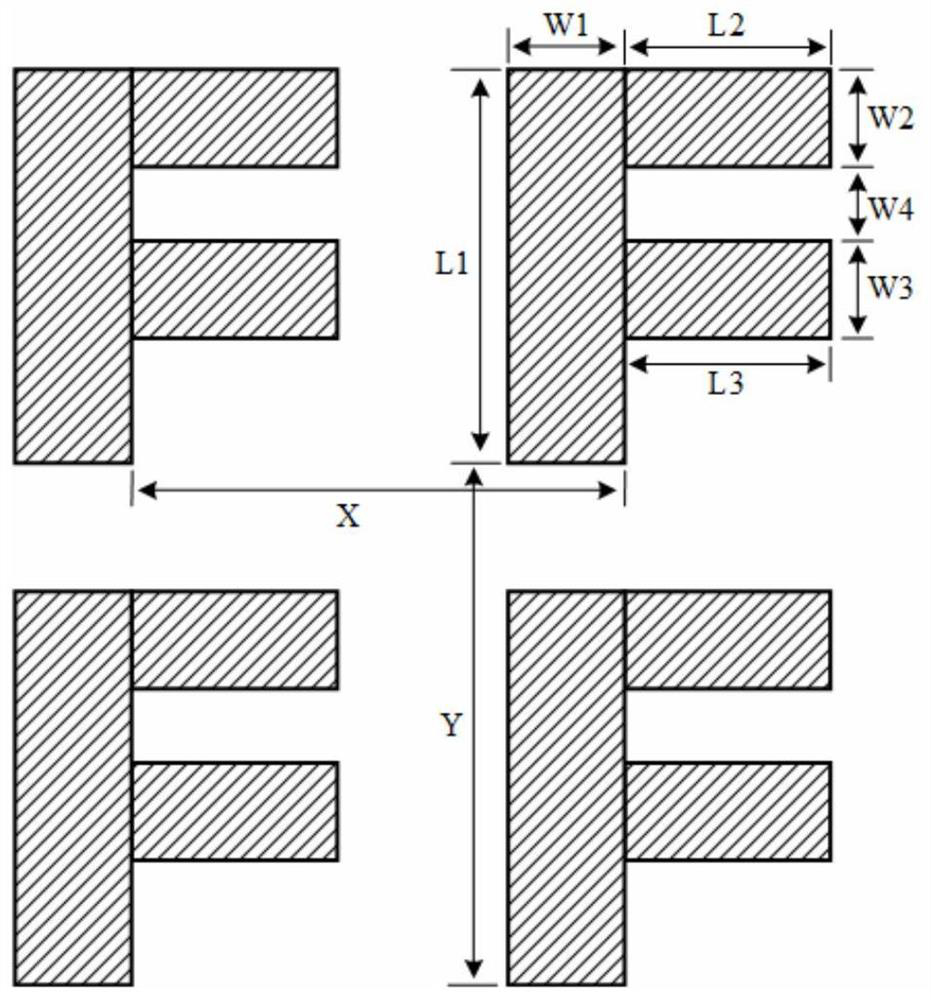
[0028] In the third step, using electron beam lithography and electron beam evaporation technology, the chiral metamaterial 4 is plated on the dielectric layer 3; where...
Embodiment 2
[0031] A microcavity with chiral polarization selectivity, such as figure 1 As shown, a substrate 1 , a metal mirror 2 , a dielectric layer 3 and a chiral metamaterial 4 are sequentially included from bottom to top. The preparation of the microcavity with chiral polarization selectivity comprises the following steps:
[0032] In the first step, a metal mirror 2 with high reflectivity is plated on the substrate 1 by electron beam evaporation technology; wherein, the material used for the substrate 1 is quartz, and the material used for the metal mirror 2 is aluminum, with a thickness of 1000nm.
[0033] In the second step, a dielectric layer 3 is plated on the metal mirror 2 by using electron beam evaporation technology; wherein, the material used for the dielectric layer 3 is titanium oxide with a thickness of 149nm.
[0034] In the third step, using electron beam lithography and electron beam evaporation technology, the chiral metamaterial 4 is plated on the dielectric layer...
PUM
| Property | Measurement | Unit |
|---|---|---|
| thickness | aaaaa | aaaaa |
| thickness | aaaaa | aaaaa |
| thickness | aaaaa | aaaaa |
Abstract
Description
Claims
Application Information
 - R&D
- Intellectual Property
- Life Sciences
- Materials
- Tech Scout
- Unparalleled Data Quality
- Higher Quality Content
- 60% Fewer Hallucinations
Browse by: Latest US Patents, China's latest patents, Technical Efficacy Thesaurus, Application Domain, Technology Topic, Popular Technical Reports.
© 2025 PatSnap. All rights reserved.Legal|Privacy policy|Modern Slavery Act Transparency Statement|Sitemap|About US| Contact US: help@patsnap.com