
LED device, manufacturing method of LED device and LED car lamp

A technology of LED devices and LED car lights, which is applied in the direction of electric solid-state devices, semiconductor devices, electrical components, etc., can solve the problems of unclear boundary between fluorescent glue and white glue, heat dissipation, scattered phosphor powder, etc., to shorten the heat radiation path, Avoid the effect of luminous dark areas and uniform luminous color

Active Publication Date: 2021-03-30
FOSHAN NATIONSTAR OPTOELECTRONICS CO LTD
View PDF9 Cites 0 Cited by
  • Summary
  • Abstract
  • Description
  • Claims
  • Application Information

AI Technical Summary

Problems solved by technology

In the above two packaging processes, due to the limitation of the process, the boundary between the fluorescent glue and the white glue is not clear, and the boundary between the two will be uneven or the phosphor powder will be scattered, which will affect the spatial distribution uniformity of the light emitting color of the lamp bead, and even It will produce obvious light-emitting dark areas and reduce the light quality of LED devices
In addition, some high-power LED devices also have heat dissipation problems. Long-term use of LED devices in high-temperature environments will lead to a decrease in their life, which is not conducive to the use and maintenance of equipment.

Method used


Image

  • LED device, manufacturing method of LED device and LED car lamp
  • LED device, manufacturing method of LED device and LED car lamp
  • LED device, manufacturing method of LED device and LED car lamp

Examples


Embodiment Construction

[0042] In order to make the technical problems solved by the present invention, the technical solutions adopted and the technical effects achieved clearer, the technical solutions of the embodiments of the present invention will be further described in detail below in conjunction with the accompanying drawings. Obviously, the described embodiments are only the technical solutions of the present invention. Some, but not all, embodiments. Based on the embodiments of the present invention, all other embodiments obtained by those skilled in the art without creative efforts fall within the protection scope of the present invention.

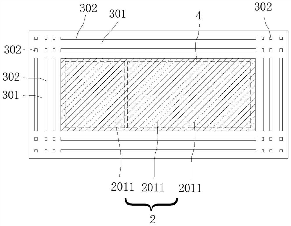
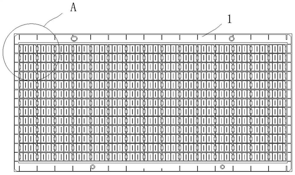
[0043] Such as figure 1 and figure 2 As shown, a LED device provided by the present invention includes a substrate 1, the substrate 1 has a mounting side 101, at least one set of chipset 2 is arranged on the mounting side 101, and the outer peripheral ring of the chipset 2 is provided with white glue to form a white glue layer 3 The chip group 2 is ...


PUM


Abstract

The present invention discloses an LED device, a manufacturing method of the LED device and an LED car lamp, wherein the LED device comprises a substrate, the substrate is provided with an installation side surface, and at least one chipset is arranged on the installation side surface; a white glue layer is annularly arranged at the periphery of each chipset, a fluorescent layer is arranged at theside, away from the substrate, of each chipset, and each white glue layer is provided with a first side surface away from the substrate. The fluorescent layer is provided with a second side surface away from the chipset, the first side surface is lower than the second side surface, and at least one first groove is concavely formed in the first side surface. The first side surface is arranged to be lower than the second side surface, so that the boundary between the white glue layer and the fluorescent layer is clear, the generation of a light-emitting dark area is avoided, the light-emittingcolor of the LED device is more uniform, the heat radiation path of a chip in the chipset and the external air can be shortened, and the heat dissipation performance of the LED device is improved; byarranging the first groove, the surface area of the first side surface can be increased, so that the surface area of outward heat radiation of the white glue layer is increased, and the heat dissipation performance of the LED device is further improved.

Description

technical field [0001] The invention relates to the technical field of LEDs, in particular to an LED device, a manufacturing method of the LED device and an LED vehicle lamp containing the LED device. Background technique [0002] At present, there are two packaging processes for LED devices, one is to fix the chip on the ceramic substrate, stick a fluorescent adhesive film on the chip, and then dot white glue around the chip to complete the package; the other is to fix the chip on the ceramic substrate Finally, dot white glue around the chip first, and then spray fluorescent glue on the chip and white glue to complete the package. In the above two packaging processes, due to the limitation of the process, the boundary between the fluorescent glue and the white glue is not clear, and the boundary between the two will be uneven or the phosphor powder will be scattered, which will affect the spatial distribution uniformity of the light emitting color of the lamp bead, and even...

Claims


Application Information

Patent Timeline
Patent Type & Authority Applications(China)
IPC IPC(8): H01L33/54H01L33/50H01L33/64H01L25/075
CPCH01L33/54H01L33/505H01L33/642H01L25/0753H01L2933/0041H01L2933/005
Inventor 陈刚范正龙李福海
Owner FOSHAN NATIONSTAR OPTOELECTRONICS CO LTD
Learn More