Method for manufacturing CMOS image sensor

a manufacturing method and image sensor technology, applied in the direction of electrical equipment, semiconductor devices, radio frequency control devices, etc., can solve the problems of lowering the uniformity of size and height, difficult to measure a critical dimension (cd), and the quantity of light approaching the photo-diode region, so as to increase the focal distance of light and light quantity, the effect of constant heigh

Active Publication Date: 2005-05-12
INTELLECTUAL VENTURES II
View PDF5 Cites 20 Cited by
  • Summary
  • Abstract
  • Description
  • Claims
  • Application Information

AI Technical Summary

Benefits of technology

[0012] The present invention is designed in consideration of the problems of the prior art, and therefore it is a primary object of the present invention to provide a method for manufacturing an image sensor which makes the boundaries between the microlenses clear by forming a guide layer in advance and can increase the focal distance of light and the quantity of light by forming the spheres of the microlenses to maintain a constant height.
[0013] It is another object of the present invention to provide a method for manufacturing a CMOS image sensor which makes a color filter array free of the topology of passivation by preserving a planarization process (an overcoating layer) as it is simply by an overcoating layer resist patterning process without accompanying etching and removal processes and which makes it easier to control the size of the color filter array.

Problems solved by technology

In case of forming a microlens with a size of less than 4 μm by the method as shown in FIG. 1, it is problematic in that the uniformity of size and height is lowered due to the inaccuracy of the boundary portions of the edges.
Moreover, it is difficult to measure a critical dimension (CD) due to the inaccuracy of a pattern, and the quantity of light approaching the photo-diode region is lowered due to the instability of the process.
Furthermore, it is difficult to adjust the thickness of a CFA and the CD size of the CFA due to the non-uniformity of the sub-topology upon forming of the CFA layer 14, thereby making the process unstable.
Accordingly, the quantity of the image converted into an electric signal is decreased or becomes non-uniform, thus the image properties of the image sensor device are deteriorated and the sensor function is also deteriorated.
Further, although an etching process has been often employed in order to overcome the circumstance similar to the above-mentioned problem, this is such a process against the reduction of defects and this increases the number of process steps and becomes disadvantageous in terms of cost saving.

Method used


Image

  • Method for manufacturing CMOS image sensor
  • Method for manufacturing CMOS image sensor
  • Method for manufacturing CMOS image sensor

Examples


Embodiment Construction

[0018] Hereinafter, a preferred embodiment of the present invention will be described in more detail referring to the drawings. In addition, the following embodiment is for illustration only, not intended to limit the scope of the invention.

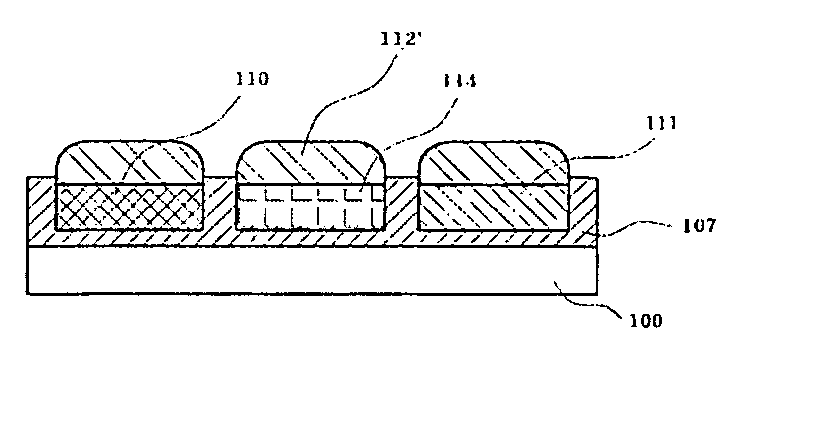
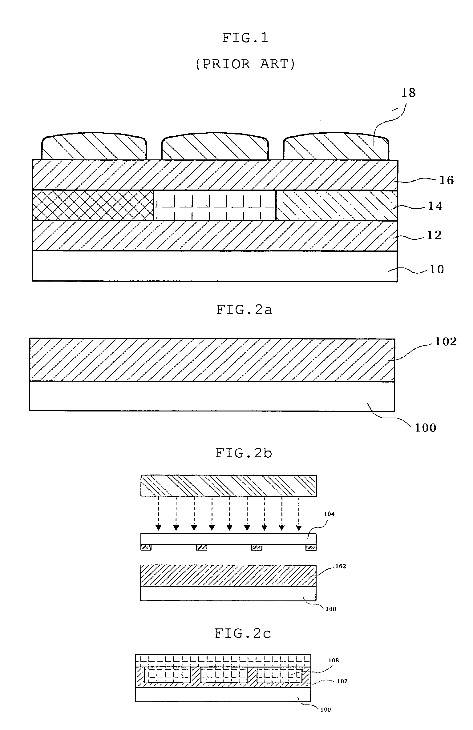
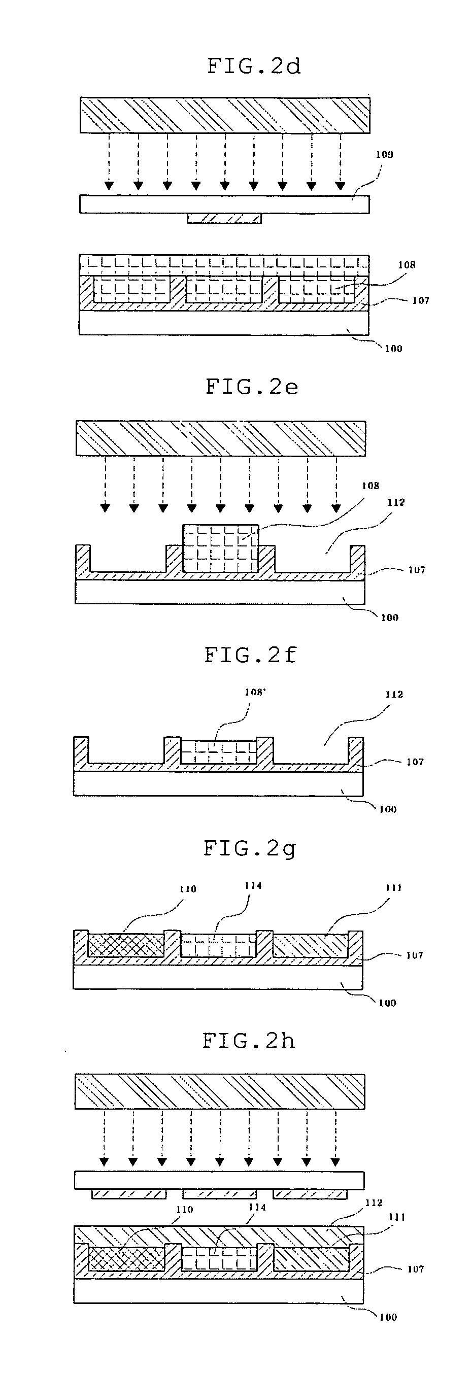
[0019]FIGS. 2a to 2i are sectional views for showing a method for manufacturing a CMOS image sensor according to a preferred embodiment of the present invention.

[0020] Firstly, as shown in FIG. 2a, an overcoating layer photoresist 102 is formed on a semiconductor substrate 100 on which a shallow trench isolation and a passivation are formed.

[0021] According to the preferred embodiment of the present invention, a color filter array device composed of blue, red and green pixels representing colors on the device is formed with a 3.2 μm×3.2 μm size. In order to maximize the function of a CFA device by increasing the quantity of external light, a microlens is formed of a photosensitive photoresist of a silicon oxide based having a high transmittanc...


PUM


Abstract

The present invention discloses a method for manufacturing an image sensor which makes the boundaries between microlenses clear by forming a guide layer in advance and can increase the focal distance of light and the quantity of light by forming the spheres of the microlenses to have a constant height.

Description

BACKGROUND OF THE INVENTION [0001] 1. Field of the Invention [0002] The present invention relates to a method for manufacturing an image sensor, and more particularly, to a method for manufacturing a CMOS image sensor which can maximize the color filter array effect of a CMOS image sensor and achieve simplification and stabilization of the process. [0003] 2. Description of the Related Art [0004] Generally, a microlens is formed in order to maximize the effect of the color filter array (CFA) of a CMOS image sensor. Such a microlens is shaped by coating a photosensitive photoresist of silicon oxides based having high light transmittance by a spin-on coating machine, patterning the same by use of a mask, and curing the same by thermally flowing it. [0005]FIG. 1 is a sectional view for showing a CMOS image sensor formed according to one of conventional techniques. [0006] As shown in FIG. 1, a semiconductor device with a color filter and a microlens includes a semiconductor substrate 10 ...

Claims


Application Information

Patent Timeline
Patent Type & Authority Applications(United States)
IPC IPC(8): H01L27/146H01L21/00
CPCH01L27/14685H01L27/146
Inventor KIM, HONG-IK
Owner INTELLECTUAL VENTURES II
Why Eureka
Try Eureka