Colors only process to reduce package yield loss

a technology of package yield and color, applied in the direction of optics, radio frequency control devices, instruments, etc., can solve the problems of large and costly systems, inferior spatial resolution, and significant improvement in size and cos

Inactive Publication Date: 2005-06-09
TAIWAN SEMICON MFG CO LTD
View PDF12 Cites 6 Cited by
  • Summary
  • Abstract
  • Description
  • Claims
  • Application Information

AI Technical Summary

Benefits of technology

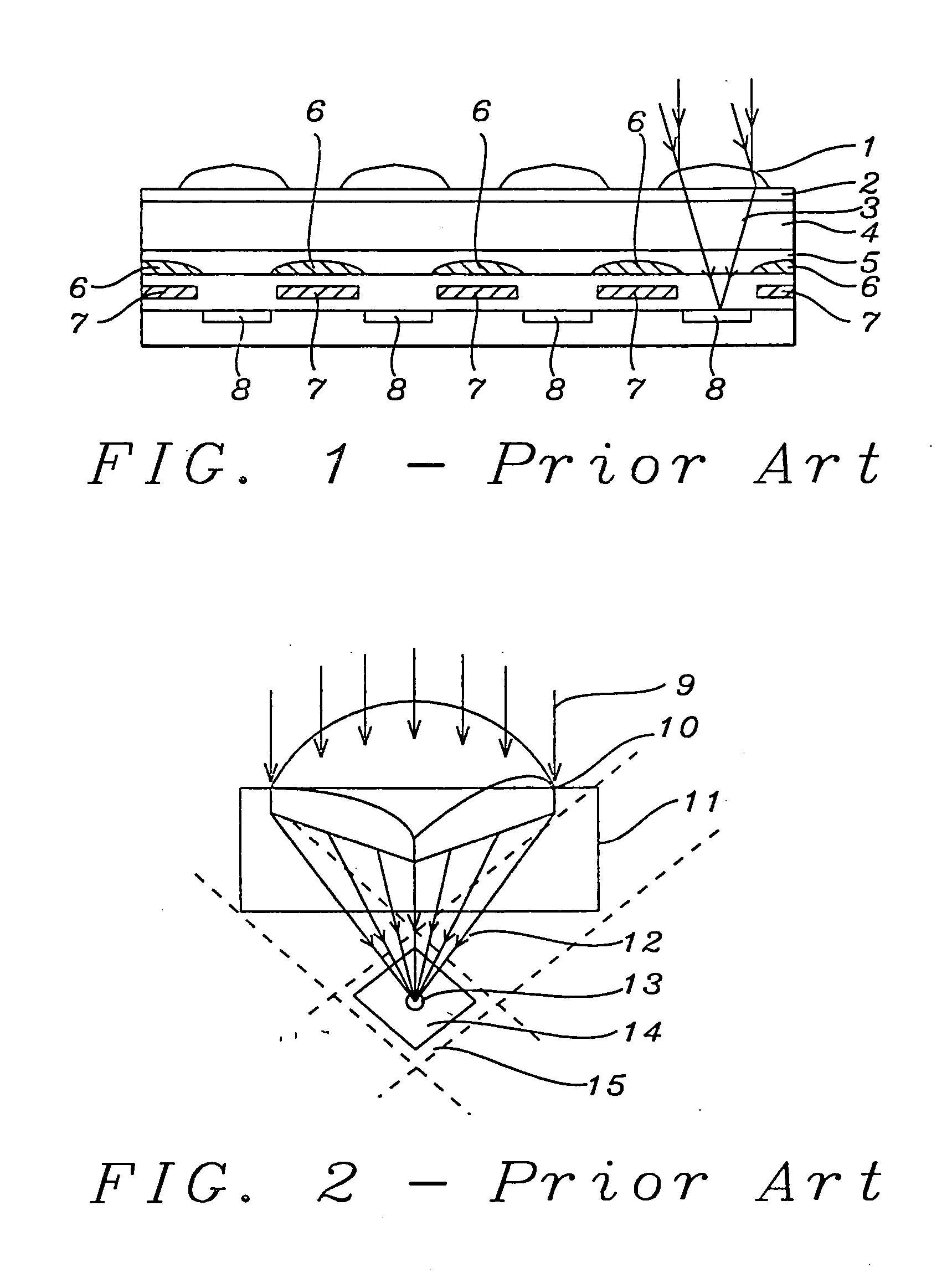
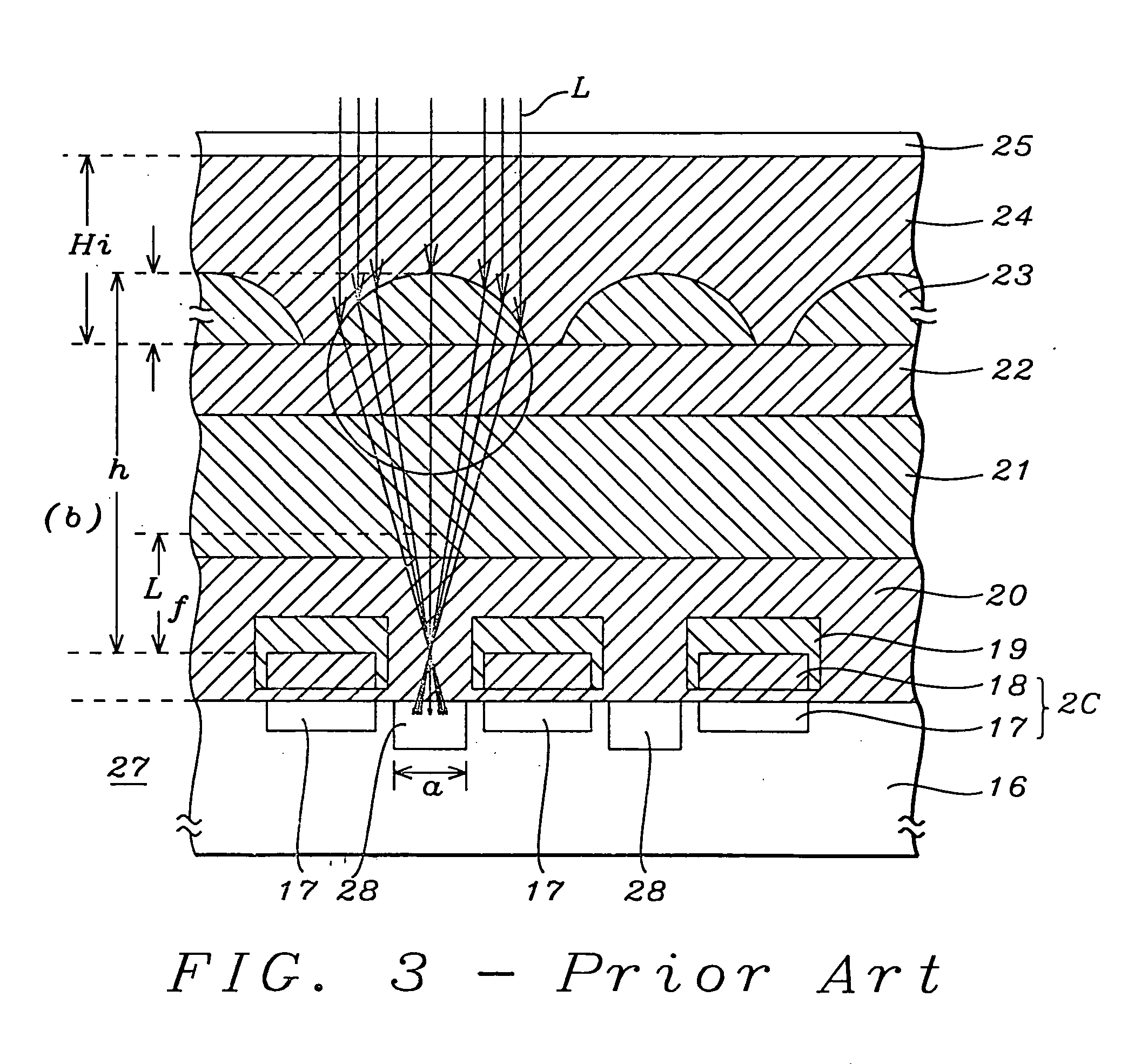
[0011] The optical performance of semiconductor imaging arrays depends on pixel size and the geometrical optical design of the camera lens, microlenses, color filter combinations, spacers, and photodiode active area size and shape. The function of the microlens is to efficiently collect incident light falling within the acceptance cone and refract this light in an image formation process onto a focal plane at a depth defined by the planar array of photodiode elements. Significant depth of focus may be required to achieve high resolution images and superior spectral signal contrast since the typical configuration positions the microlens array at the top light collecting surface and the photosensors at the semiconductor substrate surface.
[0014] The limiting numerical aperture or f-stop of the imaging camera's optical system is determined by the smallest aperture element in the convolution train. Typically, the microlens will be the limiting aperture in video camera systems. Prior Art is characterized by methods and structures to maximize the microlens aperture by increasing the radius of curvature, employing lens materials with increased refractive index, or, using compound lens arrangements to extend the focal plane deeper to match the multilayer span required to image light onto the buried photodiodes at the base surface of the semiconductor substrate. Light falling between photodiode elements or on insensitive outer zones of the photodiodes, known as dead zones, may cause image smear or noise. With Industry trends to increased miniaturization, smaller photodiodes are associated with decreasing manufacturing cost, and, similarly, mitigate against the extra steps of forming layers for Prior Art compound lens arrangements to gain increased focal length imaging. Since the microlens is aligned and matched in physical size to shrinking pixel sizes, larger microlens sizes are not a practical direction. Higher refractive index materials for the microlens would increase the reflection-loss at the air-microlens interface and result in decreased light collection efficiency and reduced spectral signal contrast or reduced signal-to-noise ratio. Limits to the numerical aperture value of the microlens are imposed by the inverse relationship of the depth of focus decreasing as the square of the numerical aperture, a strong quadratic sensitivity on the numerical aperture.

Problems solved by technology

The principal challenge in the design of solid-state color camera devices is the trade-off between adding complexity and steps to the microelectronic fabrication process wherein color filters are integrally formed in the semiconductor cross-sectional structure versus adding complexity and integrated electronic circuitry for conversion of the optical analog signals into digital form and signal processing with color-specific automated gain-control amplifiers requiring gain-ratio balance.
While color image formation may be accomplished by recording appropriately filtered images using three separate arrays, such systems tend to be large and costly.
Cameras in which a full color image is generated by a single detector array offer significant improvements in size and cost but have inferior spatial resolution.
Commercial camcorders use a process similar to this to generate a color image but typically utilize more complicated mosaic-filter designs.
Truncation of illuminance patterns falling outside the microlens aperture results in diffractive spreading and clipping or vignetting, producing undesirable nonuniformities and a dark ring around the image.
Light falling between photodiode elements or on insensitive outer zones of the photodiodes, known as dead zones, may cause image smear or noise.
Since the microlens is aligned and matched in physical size to shrinking pixel sizes, larger microlens sizes are not a practical direction.
Higher refractive index materials for the microlens would increase the reflection-loss at the air-microlens interface and result in decreased light collection efficiency and reduced spectral signal contrast or reduced signal-to-noise ratio.
The design challenge for creating superior solid-state color imagers is, therefore, to optimize spectral collection efficiency to maximize the fill-factor of the photosensor array elements without vignetting (losses from overfilling) and associated photosensor cross-talk, and, with the minimum number of microelectronic fabrication process steps.
During the package dicing step, residue particles remain embedded as a result of the topographical problem.
The resulting entrapped residue particles impact the image quality and cause yield loss of CMOS / CCD image sensor products.
Results of embedded particulates will lead to light scattering noise effects.
This coaxial cylindrical arrangement can, as Furumiya states, be subject to reflection losses at the boundary between the planarizing resin layers.
The principal problem Akio addresses is for low light levels the camera's aperture stop must be fully opened.
Under these conditions, conventional solid-state imagers will truncate or vignette significantly, diminishing their optical sensitivity.
Conventional processes for polycide-gate or salicide-gate MOS devices generally introduce the problem of inherently forming opaque regions preventing image light from entering the photosensitive regions of the silicon at a distance below the surface.
As noted previously, Kang does not address the color formation process and his optical arrangements will not operate without a converging microlens.
Prior Art is well known to have step-height or steric effect variations between R / G / B layers and results in departures from designer's specifications in transmittance color-balance.

Method used


Image

  • Colors only process to reduce package yield loss
  • Colors only process to reduce package yield loss
  • Colors only process to reduce package yield loss

Examples


Embodiment Construction

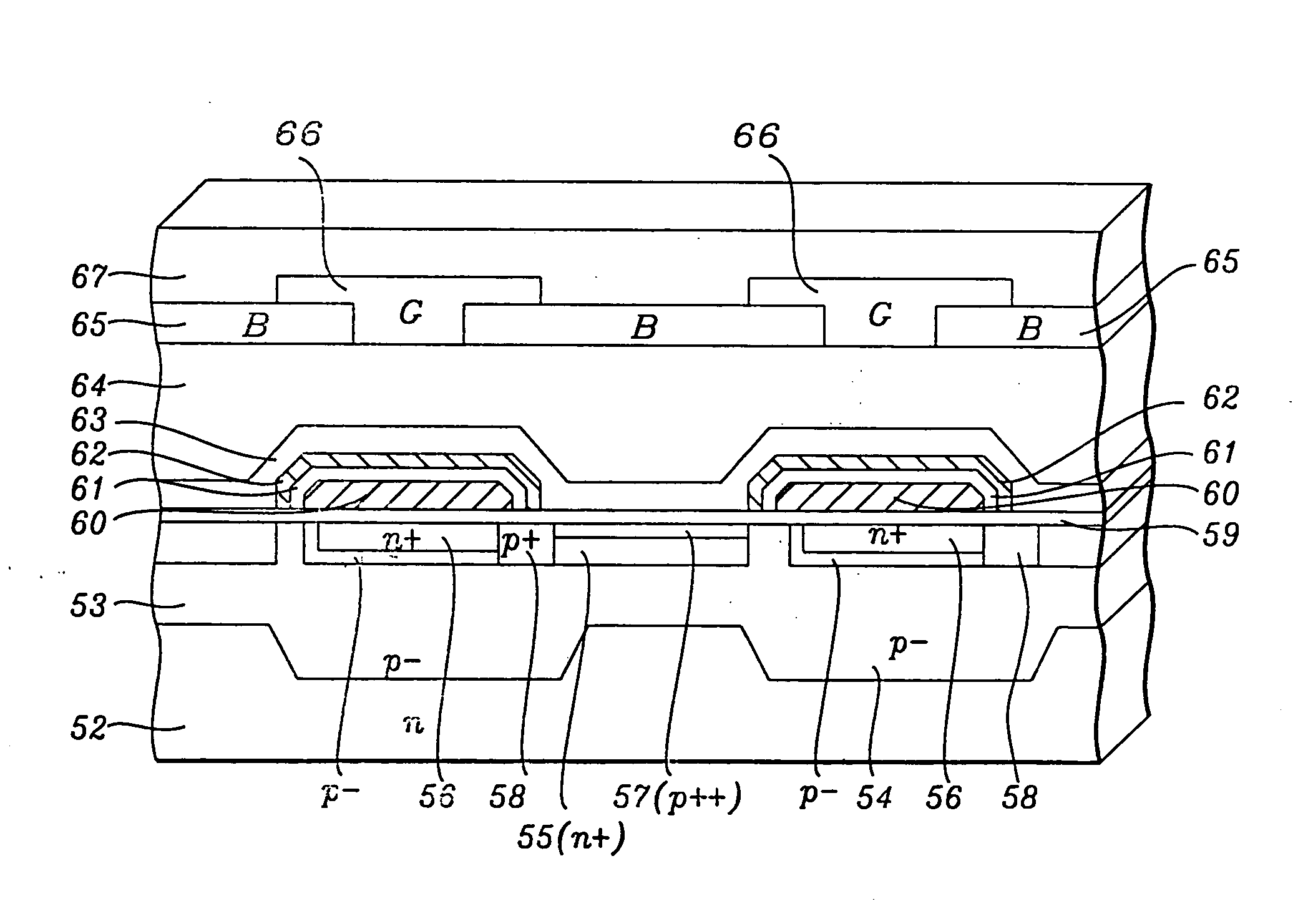
[0049] The present invention discloses a significantly simplified fabrication sequence and the specific optical conditions and materials' properties to be satisfied in forming a planar film layer of high transmittance material over at least one layer of color filters to enable high efficiency integrated semiconductor array color imaging devices without microlenses.

[0050]FIG. 5A and FIG. 5B depicts the simplified comparative fabrication flow-charts of the new process of the present invention which distinguish it from the sequence of the Prior Art process. In accord with the flow-charts shown, the manufacturing method of the present invention teaches priority formation of a high transmittance planarizing layer directly above a color filter layer residing above the sensor elements of the matrix array comprising the semiconductor imager. In the Prior Art process exhibited in FIG. 5A option 1 deposits planarization layer 47 prior to color filter formation 48. In FIG. 5A option 2 elimina...


PUM

PropertyMeasurementUnit
index of refractionaaaaaaaaaa
coloraaaaaaaaaa
areaaaaaaaaaaa

Abstract

Disclosed is an ordered microelectronic fabrication sequence in which color filters are formed by conformal deposition directly onto a photodetector array of a CCD, CID, or CMOS imaging device to create a concave-up pixel surface, and, overlayed with a high transmittance planarizing film of specified index of refraction and physical properties which optimize light collection to the photodiode without additional conventional microlenses. The optically flat top surface serves to encapsulate and protect the imager from chemical and thermal cleaning treatment damage, minimizes topographical underlayer variations which would aberrate or cause reflection losses of images formed on non-planar surfaces, and, obviates residual particle inclusions induced during dicing and packaging. A CCD imager is formed by photolithographically patterning a planar-array of photodiodes on a semiconductor substrate. The photodiode array is provided with metal photoshields, passivated, and, color filters are formed thereon. A transparent encapsulant is deposited to planarize the color filter layer and completes the solid-state color image-forming device without conventional convex microlenses.

Description

CROSS REFERENCE TO RELATED APPLICATION [0001] This is a continuation of co-pending U.S. non-provisional patent application Ser. No. 10 / 272,136, filed Oct. 16, 2002, by Fan et al., titled “Colors Only Process to Reduce Package Yield Loss,” which is a divisional application of U.S. nonprovisional patent application Ser. No. 09 / 867,379, filed May 30, 2001, by Fan et al., titled “Colors Only Process to Reduce Package Yield Loss,” now issued as U.S. Pat. No. 6,482,669, the entire contents of which are incorporated herein by reference.BACKGROUND OF THE INVENTION [0002] (1) Field of the Invention [0003] The present invention relates to light collection efficiency and package yield improvements for the optical structure and microelectronic fabrication process of semiconductor color imaging devices. [0004] (2) Description of Prior Art [0005] Synthetic reconstruction of color images in solid-state analog or digital video cameras is conventionally performed through a combination of an array of...

Claims


Application Information

Patent Timeline
Patent Type & Authority Applications(United States)
IPC IPC(8): G02F1/1335H01L21/00H01L27/146H01L31/0216H01L31/0232
CPCH01L27/14621H01L27/14623H01L27/14627H01L31/0232H01L27/14685H01L31/02162H01L27/14645H01L31/02327
Inventor FAN, YANG-TUNGPENG, CHION-SHIANCHU, CHENG-YULIN, SHIH-JANECHEN, YEN-MINGFAN, FU-JIERLIN, KUO-WEI
Owner TAIWAN SEMICON MFG CO LTD
Why Eureka
Try Eureka