Spherical grid array package

An array packaging and ball grid technology, which is applied in the direction of printed circuits, electrical components, and electrical solid devices connected with non-printed electrical components, and can solve problems such as limitations and difficulties in implementation.

Inactive Publication Date: 2003-10-29
MAGNACHIP SEMICONDUCTOR LTD
View PDF0 Cites 1 Cited by
  • Summary
  • Abstract
  • Description
  • Claims
  • Application Information

AI Technical Summary

Problems solved by technology

In order to solve this problem, the diameter of the ball must be reduced,

Method used


Image

  • Spherical grid array package
  • Spherical grid array package
  • Spherical grid array package

Examples


Embodiment Construction

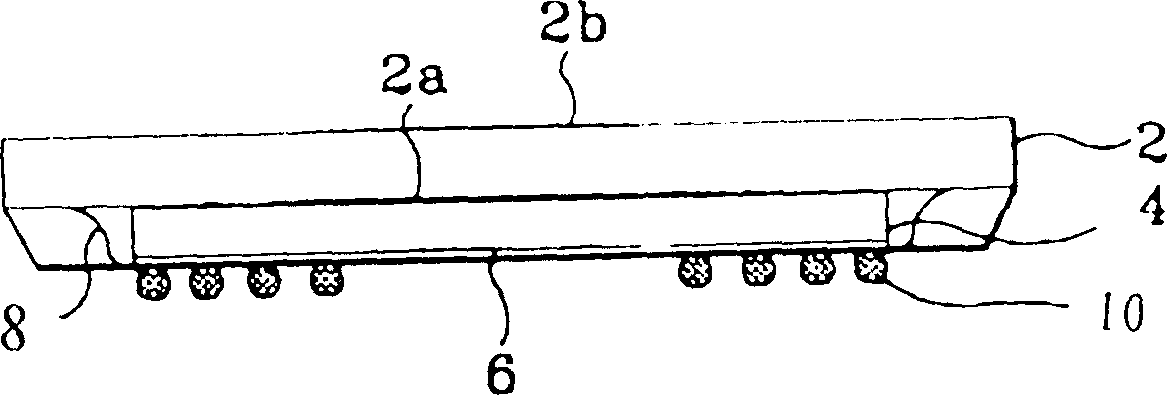
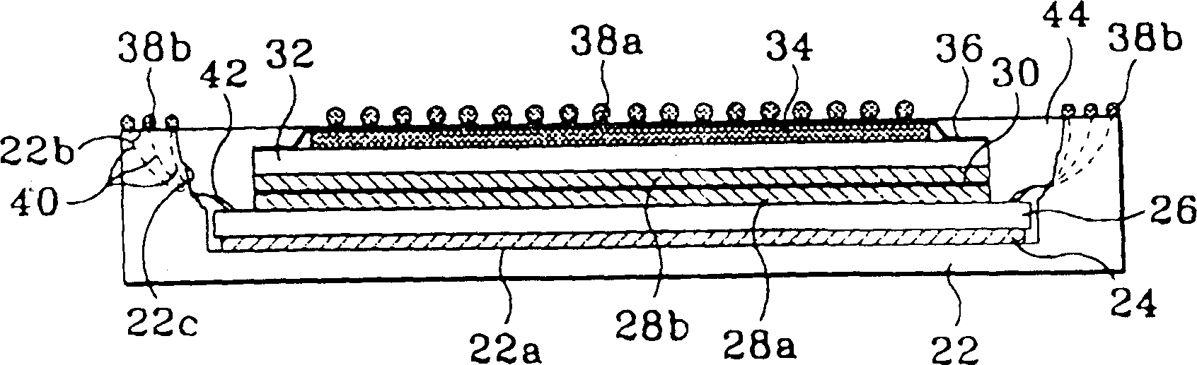
[0012] figure 1 It is a schematic cross-sectional view of a representative micro ball grid array (μ-Ball Grid Array: μ-BGA) in the conventional chip scale package (Chip Scale Package) group.

[0013] refer to figure 1 , a semiconductor chip 2 is provided, that is, a die, which has an inner surface 2a and an outer surface 2b, a plurality of semiconductor elements are formed on the inner surface 2a, and a plurality of semiconductor elements are formed on the upper surface of the inner surface 2a for communicating with the outside Bonding points (not shown) where the circuit passes signals. These bonding points are formed at the ends of the semiconductor chip 2 . exist figure 1 In this case, the inner surface 2a of the semiconductor chip 2 faces downward. On the inner surface 2a of the semiconductor chip 2, an elastic rubber 4 and a flexible beam lead film 6 printed with circuit wiring are laminated in this order. Next, the elastic rubber 4 and the beam lead film 6 will be d...


PUM


Abstract

An improved ball grid array package BGA, which can prevent the impact between solder balls and improve integration, includes: a substrate with a first surface and a second surface higher than the first surface; at least one semiconductor chip, which is Stacked and arranged on the first surface, a plurality of pads are provided on the upper surface; a plurality of leads are provided on the substrate, one end of which is connected to a part of the pads of the semiconductor chip, and the other end is exposed on the second surface On: a plurality of conductive solder balls are formed on the surface of the semiconductor chip and the second surface of the substrate, and are electrically connected to the pads of the semiconductor chip and the leads exposed on the second surface of the substrate.

Description

technical field [0001] The invention relates to a ball grid array package, in particular to a miniature ball grid array package with an improved ball configuration structure. Background technique [0002] With the rapid development of integrated circuit manufacturing processes, packaging technology for protecting many unit elements formed on a unit chip from external environments has also been developed along with other manufacturing technologies. In most electronic devices, packaged semiconductor chips are mounted, and efforts have been made to minimize the area of ​​printed circuit boards on which such semiconductor chips are mounted, and miniaturization of package sizes has been demanded in response to such efforts. As one of technologies for miniaturizing the package size, a chip size package (Chip Size Package: CSP) or a chip scale package (Chip Scale Package: CSP) has been proposed, which reduces the size of the package to a level equivalent to the chip size. Among su...

Claims


Application Information

Patent Timeline
IPC IPC(8): H01L23/12H01L23/055H01L25/065H01L25/07H01L25/18H05K1/18
CPCH01L23/055H01L25/0657H01L2225/0651H01L2225/06517H01L2225/06582H01L2225/06586H01L2924/01079H01L24/49H01L2224/48091H01L2224/48227H01L2224/49109H01L2224/49175H01L2224/49433H01L2224/73265H01L2924/00014H01L2924/14H01L24/48H01L2224/45099H01L2224/05599H01L2924/00H05K1/18
Inventor 南泽焕
Owner MAGNACHIP SEMICONDUCTOR LTD
Why Eureka
Try Eureka