Middle frame of electronic equipment, manufacturing method of middle frame, shell of electronic equipment and electronic equipment

A technology of electronic equipment and production method, which is applied to branch equipment, telephone communication, electrical components, etc., can solve the problems of lowering the degree of vividness and brightness of colors, unable to achieve the brilliant effect of pink and gold, and expensive gold.

Active Publication Date: 2021-04-09
SHENZHEN YUNMI C CRPTOLOG COMM TECH CO LTD
View PDF7 Cites 0 Cited by
  • Summary
  • Abstract
  • Description
  • Claims
  • Application Information

AI Technical Summary

Problems solved by technology

However, because the metal layer will interfere with the electronic signal and usually the plated metal includes gold, the gold itself has the problem of being expensive, so that the method of directly plating metal to obtain pink gold cannot be widely used.
In the way of spraying ink, due to the limitation of materials, the vividness and brightness of the color will be reduced, and the proportion of pink gold ink is difficult to achieve the gorgeous effect of pink gold produced by direct metal plating.

Method used


Image

  • Middle frame of electronic equipment, manufacturing method of middle frame, shell of electronic equipment and electronic equipment
  • Middle frame of electronic equipment, manufacturing method of middle frame, shell of electronic equipment and electronic equipment
  • Middle frame of electronic equipment, manufacturing method of middle frame, shell of electronic equipment and electronic equipment

Examples


preparation example Construction

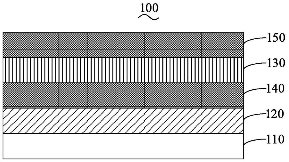
[0053] The preparation process of the first UV adhesive layer 140 includes: the pre-baking temperature is 50°C-60°C, the pre-baking time is 3min-5min; the humidity of the spray booth is 45%-70%, and the temperature of the spray booth is 18°C-25°C; The irradiation energy of the furnace is 900mj / cm 2 ~1200mj / cm 2 . The above only lists a commonly used UV adhesive layer preparation process, but is not limited thereto, and can also be a commonly used UV adhesive layer preparation process in the art.

[0054] Further, the thickness of the first UV adhesive layer 140 is 8 μm˜12 μm. In one embodiment, the thickness of the first UV adhesive layer 140 is 8 μm, 9 μm, 10 μm, 11 μm or 12 μm.

[0055] The function of the second UV adhesive layer 150 is mainly to protect the optical film layer 130 and improve the overall wear resistance of the middle frame 100 of the electronic device. The composition and preparation process of the second UV adhesive layer 150 are the same as those of t...

Embodiment 1

[0094] The manufacturing process of the middle frame of the electronic device in this embodiment is specifically as follows:

[0095] (1) Spray coating on the substrate to form a coating layer with a thickness of 16 μm. Wherein, the raw material of the paint layer is composed of paint main agent and 783 slow-drying water (thinner) with a mass ratio of 1:3. In terms of parts by mass, the paint main agent consists of 20 parts of ABS resin, 30 parts of naphthol red and silver powder (pigment) with a mass ratio of 1:1, 30 parts of 783 slow-drying water (solvent) and 2 parts of dispersant (auxiliary) portion composition.

[0096] (2) Form a first UV adhesive layer with a thickness of 12 μm on the side of the coating layer away from the substrate. The raw material of the first UV adhesive layer consists of 783 slow-drying water (thinner), photoinitiator and defoamer with a mass ratio of 50:50:2.

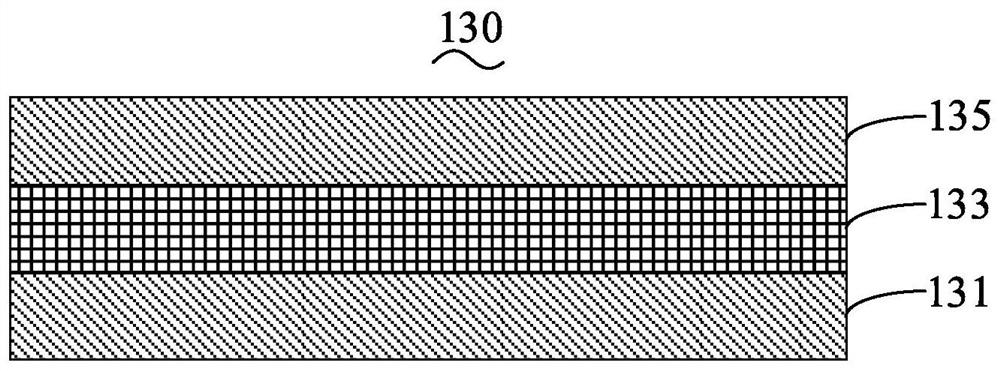
[0097] (3) Sputtering sequentially on the side of the first UV glue layer away from...

Embodiment 2

[0100] The manufacturing process of the middle frame of the electronic device in this embodiment is specifically as follows:

[0101] (1) Spray coating on the substrate to form a coating layer with a thickness of 16 μm. Wherein, the raw material of the paint layer is composed of paint main agent and 783 slow-drying water (thinner) with a mass ratio of 1:3. In terms of parts by mass, the paint main agent consists of 20 parts of ABS resin, 30 parts of naphthol red and silver powder (pigment) with a mass ratio of 1:1, 30 parts of 783 slow-drying water (solvent) and 2 parts of dispersant (auxiliary) portion composition.

[0102] (2) Form a first UV adhesive layer with a thickness of 12 μm on the side of the coating layer away from the substrate. The raw material of the first UV adhesive layer consists of 783 slow-drying water (thinner), photoinitiator and defoamer with a mass ratio of 50:50:2.

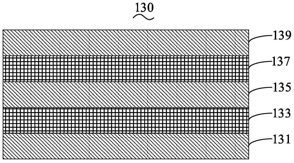
[0103] (3) Form the first high-refractive index layer, the first low-refractive-ind...


PUM

PropertyMeasurementUnit
Thicknessaaaaaaaaaa
Thicknessaaaaaaaaaa
Thicknessaaaaaaaaaa

Abstract

The invention relates to a middle frame of electronic equipment, a manufacturing method of the middle frame, a shell of the electronic equipment and the electronic equipment. The middle frame of the electronic equipment comprises a base material, a coating layer arranged on the base material and an optical film layer arranged on the side, away from the base material, of the coating layer. The raw materials for preparing the coating layer comprise a coating main agent and a diluent, and the coating main agent comprises, by mass, 15-35 parts of resin, 20-40 parts of pigment, 25-45 parts of a solvent and 1-6 parts of auxiliaries. The optical film layer comprises at least one high-refractive-index layer and at least one low-refractive-index layer, the high-refractive-index layers and the low-refractive-index layers are alternately arranged, the outermost layer, away from the base material, of the optical film layer is a high-refractive-index layer, and the Lab color chromaticity indexes of the middle frame of the electronic equipment are as follows: L = 55-65, a = 10-20 and b = 15-30. The middle frame of the electronic equipment has a pink appearance, is high in brightness, and does not interfere with signals of the electronic equipment.

Description

technical field [0001] The invention relates to the field of electronic equipment, in particular to a middle frame of an electronic equipment and a manufacturing method thereof, a casing of the electronic equipment and the electronic equipment. Background technique [0002] With the widespread use of electronic equipment, people are constantly pursuing the high performance of electronic equipment while also pursuing a fashionable appearance. Among these fashionable appearances, the color of gold and rose is the color effect that people have been pursuing. At the same time, in the visual In effect, pink gold with gold and rose colors is a favorite color. [0003] Among the most frequently used electronic devices, mobile phones are devices that are basically used every day. In the appearance of the mobile phone, the front and rear covers are basically glass and composite boards. Different appearance colors are achieved by silk screen printing and film sticking, but glass and ...

Claims


Application Information

Patent Timeline
IPC IPC(8): C09D155/02H04M1/02
CPCC09D155/02H04M1/026H04M1/0283
Inventor 张春姣周天济
Owner SHENZHEN YUNMI C CRPTOLOG COMM TECH CO LTD
Why Eureka
Try Eureka